- 您現(xiàn)在的位置:買賣IC網(wǎng) > PDF目錄358752 > LC245A (Texas Instruments, Inc.) OCTAL BUS TRANSCEIVER WITH 3-STATE OUTPUTS PDF資料下載
參數(shù)資料
| 型號: | LC245A |
| 廠商: | Texas Instruments, Inc. |
| 英文描述: | OCTAL BUS TRANSCEIVER WITH 3-STATE OUTPUTS |
| 中文描述: | 八路總線收發(fā)器具有三態(tài)輸出 |
| 文件頁數(shù): | 7/19頁 |
| 文件大小: | 585K |
| 代理商: | LC245A |

www.ti.com
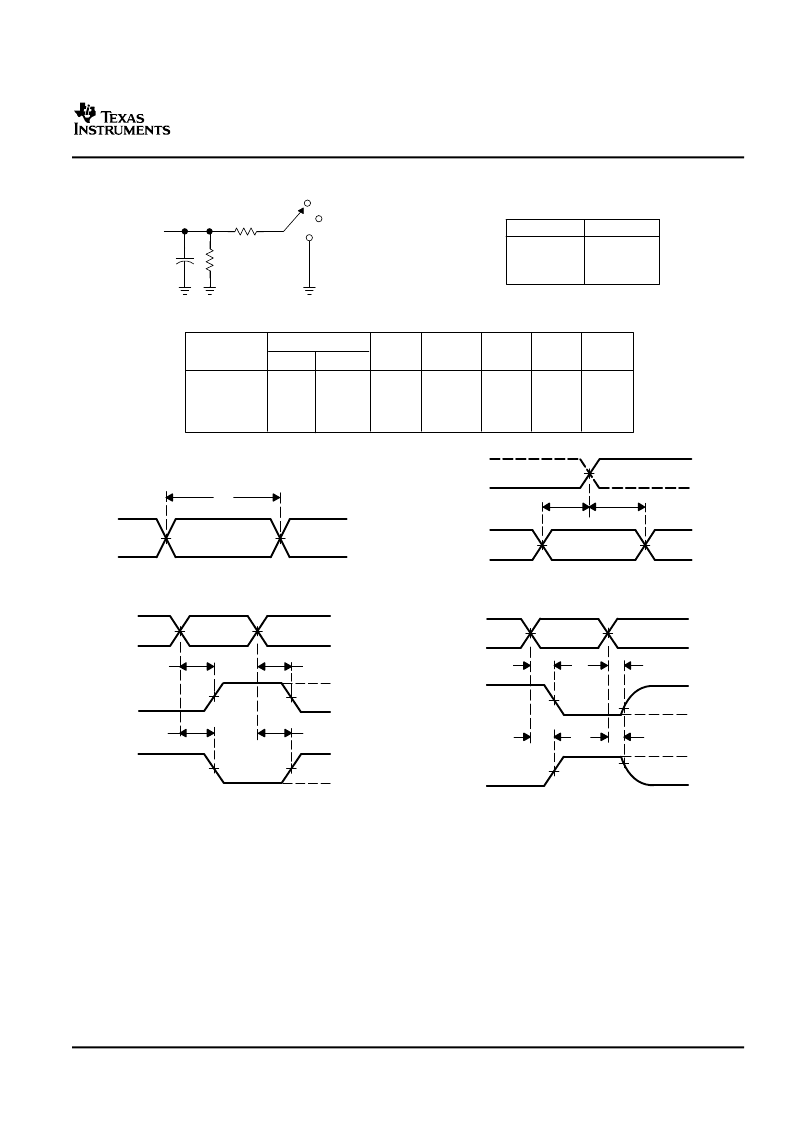
PARAMETER MEASUREMENT INFORMATION
V
M
t
h
t
su
From Output
Under Test
C
L
(see Note A)
LOAD CIRCUIT
S1
V
LOAD
Open
GND
R
L
R
L
Data Input
Timing Input
V
I
0 V
V
I
0 V
0 V
t
w
Input
VOLTAGE WAVEFORMS
SETUP AND HOLD TIMES
VOLTAGE WAVEFORMS
PROPAGATION DELAY TIMES
INVERTING AND NONINVERTING OUTPUTS
VOLTAGE WAVEFORMS
PULSE DURATION
t
PLH
t
PHL
t
PHL
t
PLH
V
OH
V
OH
V
OL
V
OL
V
I
0 V
Input
Output
Waveform 1
S1 at V
LOAD
(see Note B)
Output
Waveform 2
S1 at GND
(see Note B)
V
OL
V
OH
t
PZL
t
PZH
t
PLZ
t
PHZ
V
LOAD
/2
0 V
V
OL
+ V
V
OH
- V
≈
0 V
V
I
VOLTAGE WAVEFORMS
ENABLE AND DISABLE TIMES
LOW- AND HIGH-LEVEL ENABLING
Output
Output
t
PLH
/t
PHL
t
PLZ
/t
PZL
t
PHZ
/t
PZH
Open
V
LOAD
GND
TEST
S1
NOTES: A. C
L
includes probe and jig capacitance.
B. Waveform 1 is for an output with internal conditions such that the output is low, except when disabled by the output control.
Waveform2 is for an output with internal conditions such that the output is high, except when disabled by the output control.
C. All input pulses are supplied by generators having the following characteristics: PRR
≤
10 MHz, Z
O
= 50
.
D. The outputs are measured one at a time, with one transition per measurement.
E. t
PLZ
and t
PHZ
are the same as t
dis
.
F. t
PZL
and t
PZH
are the same as t
en
.
G. t
PLH
and t
PHL
are the same as t
pd
.
H. All parameters and waveforms are not applicable to all devices.
Output
Control
V
M
V
M
V
M
V
M
V
M
V
M
V
M
V
M
V
M
V
M
V
M
V
M
V
I
V
M
V
M
1.8 V
±
0.15 V
2.5 V
±
0.2 V
2.7 V
3.3 V
±
0.3 V
1 k
500
500
500
V
CC
R
L
2
×
V
CC
2
×
V
CC
6 V
6 V
V
LOAD
C
L
30 pF
30 pF
50 pF
50 pF
0.15 V
0.15 V
0.3 V
0.3 V
V
V
CC
V
CC
2.7 V
2.7 V
V
I
V
CC
/2
V
CC
/2
1.5 V
1.5 V
V
M
t
r
/t
f
≤
2 ns
≤
2 ns
≤
2.5 ns
≤
2.5 ns
INPUTS
SN74LVC245A
OCTAL BUS TRANSCEIVER
WITH 3-STATE OUTPUTS
SCAS218T–JANUARY 1993–REVISED FEBRUARY 2005
Figure 1. Load Circuit and Voltage Waveforms
7
相關(guān)PDF資料 |
PDF描述 |
|---|---|
| LC3011PGC-022 | High Performance, Low-Cost Analog Line Scan Camera |
| LC3011PGN-022 | High Performance, Low-Cost Analog Line Scan Camera |
| LC301 | RED OVAL LAMP LED |
| LC3101 | 128K-BIT CMOS MASK ROM |
| LC321664AT-80 | 1 MEG (65536 words X 16 bits) DRAM Fast Page Mode, Byte Write |
相關(guān)代理商/技術(shù)參數(shù) |
參數(shù)描述 |
|---|---|
| LC-2488A4E | 制造商:未知廠家 制造商全稱:未知廠家 功能描述:Telecomm/Datacomm |
| LC-2488A4E1 | 制造商:未知廠家 制造商全稱:未知廠家 功能描述:Telecommunication IC |
| LC-2488A4E1H | 制造商:未知廠家 制造商全稱:未知廠家 功能描述:Telecommunication IC |
| LC-2488A4E1T | 制造商:未知廠家 制造商全稱:未知廠家 功能描述:Telecommunication IC |
| LC-2488A4E2 | 制造商:未知廠家 制造商全稱:未知廠家 功能描述:Telecommunication IC |
發(fā)布緊急采購,3分鐘左右您將得到回復(fù)。