- 您現(xiàn)在的位置:買賣IC網(wǎng) > PDF目錄377605 > LBMG (Linear Technology Corporation) 20mA, 3V to 80V Low Dropout Micropower Linear Regulator PDF資料下載
參數(shù)資料
| 型號(hào): | LBMG |
| 廠商: | Linear Technology Corporation |
| 英文描述: | 20mA, 3V to 80V Low Dropout Micropower Linear Regulator |
| 中文描述: | 20mA的,3V至80V的微功率低壓差線性穩(wěn)壓器 |
| 文件頁數(shù): | 11/16頁 |
| 文件大?。?/td> | 194K |
| 代理商: | LBMG |
11
LT3014
3014fb
OUTPUT VOLTAGE (V)
0
R
μ
A
50
45
40
30
35
25
20
15
10
5
0
8
3014 F04
2
1
3
5
7
9
4
6
10
T
J
= 25
°
C
V
IN
= 0V
V
OUT
= V
ADJ
CURRENT FLOWS
INTO OUTPUT PIN
ADJ PIN
ESD CLAMP
APPLICATIOU
In situations where the ADJ pin is connected to a resistor
divider that would pull the ADJ pin above its 7V clamp
voltage if the output is pulled high, the ADJ pin input
current must be limited to less than 5mA. For example, a
resistor divider is used to provide a regulated 1.5V output
from the 1.22V reference when the output is forced to 60V.
The top resistor of the resistor divider must be chosen to
limit the current into the ADJ pin to less than 5mA when the
ADJ pin is at 7V. The 53V difference between the OUT and
ADJ pins divided by the 5mA maximum current into the
ADJ pin yields a minimum top resistor value of 10.6k.
In circuits where a backup battery is required, several
different input/output conditions can occur. The output
voltage may be held up while the input is either pulled to
ground, pulled to some intermediate voltage, or is left
W
U
U
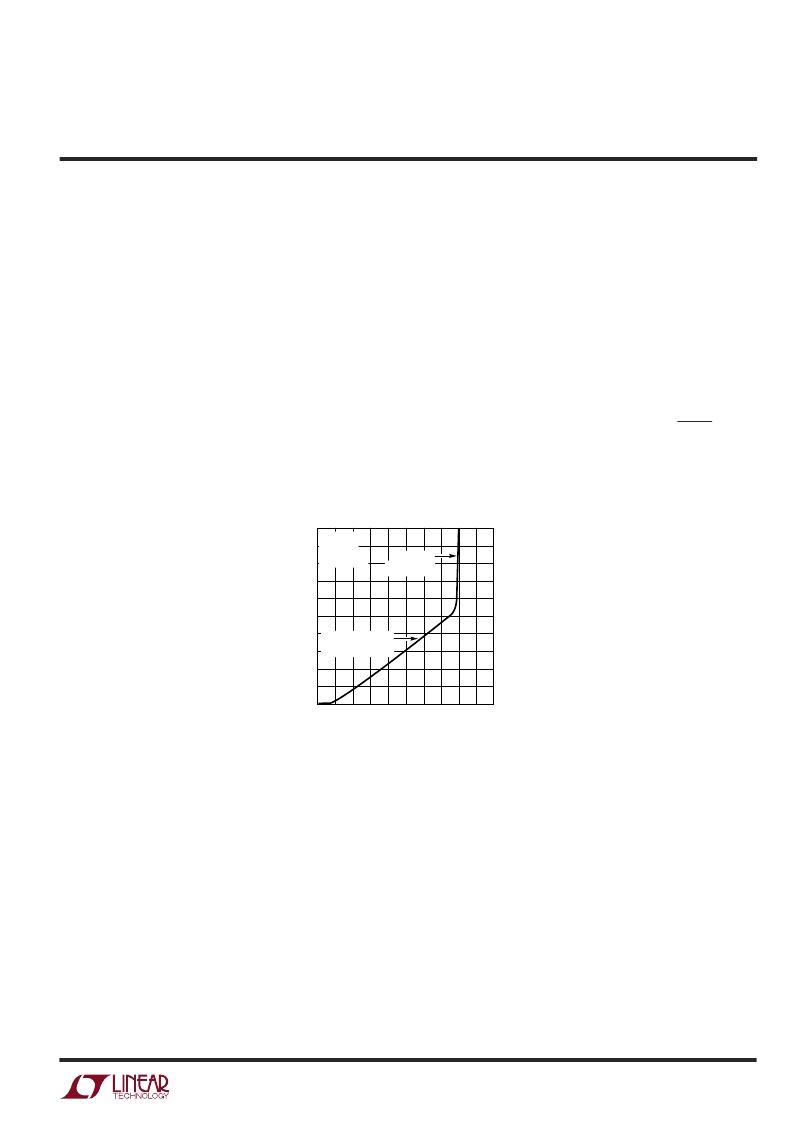
Figure 4. Reverse Output Current
open circuit. Current flow back into the output will follow
the curve shown in Figure 4. The rise in reverse output
current above 7V occurs from the breakdown of the 7V
clamp on the ADJ pin. With a resistor divider on the
regulator output, this current will be reduced depending
on the size of the resistor divider.
When the IN pin of the LT3014 is forced below the OUT pin
or the OUT pin is pulled above the IN pin, input current will
typically drop to less than 2
μ
A. This can happen if the input
of the LT3014 is connected to a discharged (low voltage)
battery and the output is held up by either a backup battery
or a second regulator circuit. The state of the SHDN pin will
have no effect on the reverse output current when the
output is pulled above the input.
相關(guān)PDF資料 |
PDF描述 |
|---|---|
| LBRT | 20mA, 3V to 80V Low Dropout Micropower Linear Regulator |
| LBMM | Precision, 100UA Gain Selectable Amplifier |
| LBN07076 | 70MHz SAW Filter 25MHz Bandwidth |
| LBN07092 | 70MHz SAW Filter 6MHz Bandwidth |
| LBN07094 | 70MHz SAW Filter 17.5MHz Bandwidth |
相關(guān)代理商/技術(shù)參數(shù) |
參數(shù)描述 |
|---|---|
| LBMM | 制造商:LINEAR 制造商全稱:LINEAR 功能描述:Precision, 100UA Gain Selectable Amplifier |
| LBMP0.0022400J7.5 | 制造商:Alpha 3 Manufacturing 功能描述: |
| LBMP0.0027400J7.5 | 制造商:Alpha 3 Manufacturing 功能描述: |
| LBMP0.0047400J7.5 | 制造商:Alpha 3 Manufacturing 功能描述: |
| LBMP0.0068400J7.5 | 制造商:Alpha 3 Manufacturing 功能描述: |
發(fā)布緊急采購,3分鐘左右您將得到回復(fù)。