- 您現在的位置:買賣IC網 > PDF目錄97997 > LB1897H BRUSHLESS DC MOTOR CONTROLLER, PDSO34 PDF資料下載
參數資料
| 型號: | LB1897H |
| 元件分類: | 運動控制電子 |
| 英文描述: | BRUSHLESS DC MOTOR CONTROLLER, PDSO34 |
| 封裝: | 0.375 INCH, HSSOP-28 |
| 文件頁數: | 4/11頁 |
| 文件大小: | 159K |
| 代理商: | LB1897H |
LB1897H
No.8804-2/11
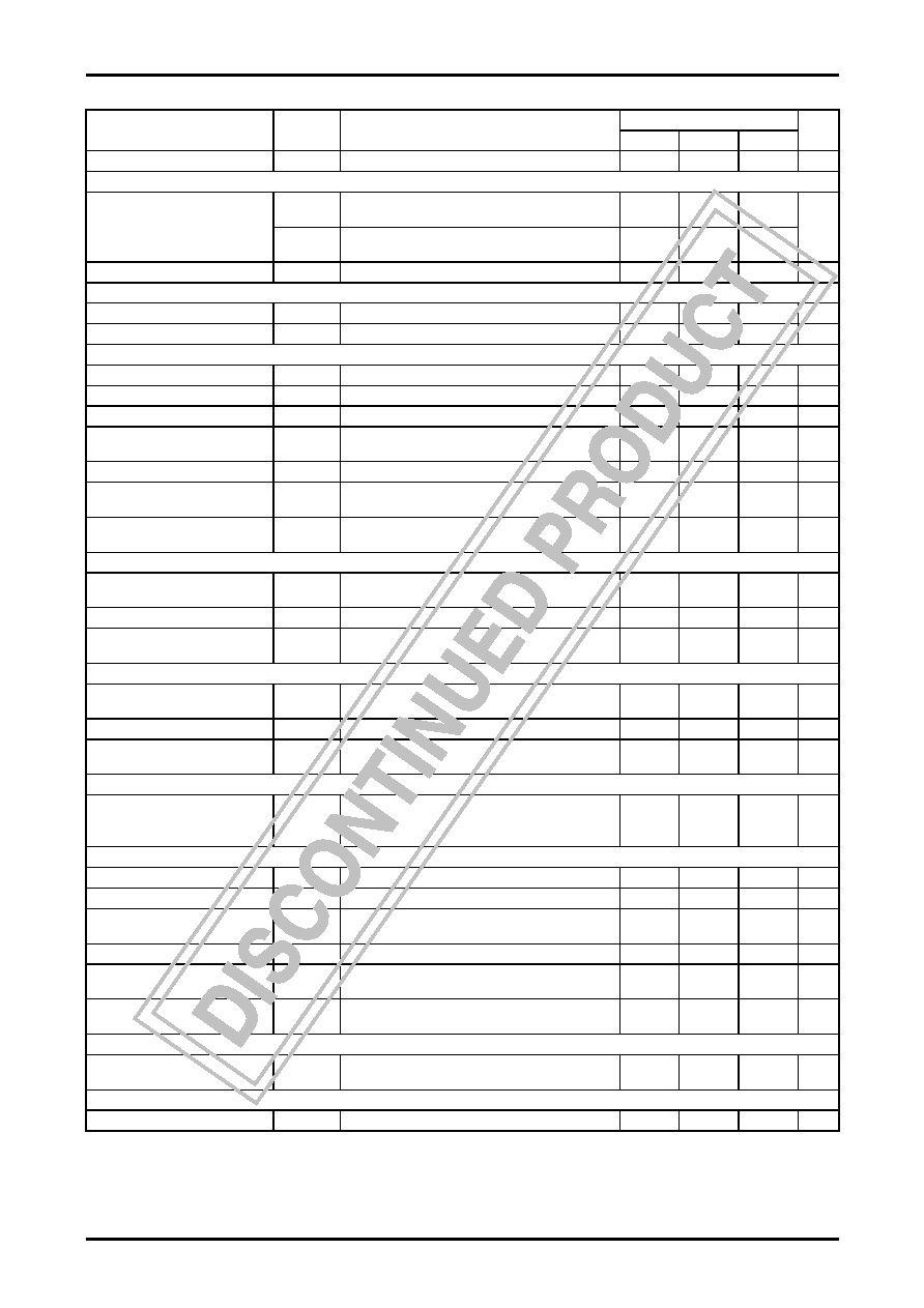
Electrical Characteristics
at Ta = 25
°C, VCC = 5V, VS = 15V
Ratings
Parameter
Symbol
Conditions
min
typ
max
Unit
VCC supply current
ICC
RL = ∞, VCTL = 0V, VLIM = 0V (at quiescence)
12
18
mA
[Output]
VOsat1
IO = 500mA, Rf = 0.5, Sink+Source
VCTL = VLIM = 5V (with over-saturation prevention)
2.1
2.6
Output saturation voltage
VOsat2
IO = 1.0A, Rf = 0.5, Sink+Source
VCTL = VLIM = 5V (with over-saturation prevention)
2.6
3.5
V
Output leak current
IOleak
1.0
mA
[FR]
FR pin input threshold voltage
VFSR
2.25
2.50
2.75
V
FR pin input input bias current
Ib (FSR)
-5.0
A
[Control]
CTLREF pin voltage
VCREF
2.37
2.50
2.63
V
CTLREF pin input range
VCREFIN
1.70
3.50
V
CTL pin input bias current
Ib (CTL)
With VCTL = 5V, CTLREF : OPEN
8.0
A
CTL pin control start voltage
VCTL (ST)
At Rf = 0.5
, VLIM = 5V, IO ≥ 10mA
With hall input logic fixed (U, V, W = H, H, L)
2.20
2.35
2.50
V
CTL pin control changeover voltage VCTL (ST2)
At Rf = 0.5
, VLIM = 5V
3.00
3.15
3.30
V
CTL pin control Gm1
Gm1 (CTL)
Rf = 0.5
, IO = 200mA
With hall input logic fixed (U, V, W = H, H, L)
0.52
0.65
0.78
A/V
CTL pin control Gm2
Gm2 (CTL)
Rf = 0.5
, VCTL = 200mV
With hall input logic fixed (U, V, W = H, H, L)
1.20
1.50
1.80
A/V
[Current limiting]
LIM current limiting offset voltage
VOFF(LIM)
Rf = 0.5
, VCTL = 5V, IO ≥ 10mA
With hall input logic fixed (U, V, W = H, H, L)
140
200
260
mV
LIM pin input bias current
Ib (LIM)
At VCTL = 5
, VCREF : OPEN, VLIM = 0V
-2.5
A
LIM pin current limiting level
Ilim
Rf = 0.5
, VCTL = 5V, VLIM = 2.06V
With hall input logic fixed (U, V, W = H, H, L)
830
900
970
mA
[Hall amp]
Hall amp input offset voltage
VOFF
(HALL)
-6
+6
mV
Hall amp input bias voltage
Ib (HALL)
1.0
3.0
A
Hall amp common input voltage
VCM
(HALL)
1.3
3.3
V
[TRC]
Torque ripple compensation ratio
TRC
At a bottom and peak of Rf waveform with IO =
200mA
(RF = 0.5
)
Note 2
9
%
[FG amplifier]
FG amp input offset voltage
VOFF(FG)
-8
+8
mV
FG amp input bias current
Ib (FG)
-100
nA
FG amp output saturation voltage
VOsat
(FG)
Sink side. At internal pull-up resistor load
0.5
V
FG amp common input voltage
VCM(FG)
0.5
4.0
V
FG amp positive side output
characteristic breakpoint
VCLIP
(POS)
+0.360
+0.450
+0.540
V
GF amp negative side output
characteristic breakpoint
VCLIP
(NEG)
-0.540
-0.450
-0.360
V
[Saturation]
Saturation preventive circuit lower
side setting voltage
VOsat
(DET)
Each OUT-Rf voltage at IO = 10mA, Rf = 0.5
VCTL = VLIM = 5V
0.175
0.25
0.325
V
[TSD]
TSD operating temperature
T-TSD
(Set target value)
Note 1
170
°C
Note 1. For the design target value in the “Conditions” column, no measurement is made.
相關PDF資料 |
PDF描述 |
|---|---|
| LB1927 | BRUSHLESS DC MOTOR CONTROLLER, 2.5 A, PDIP28 |
| LB1927 | BRUSHLESS DC MOTOR CONTROLLER, 2.5 A, PDIP28 |
| LB8108M | DISK DRIVE MOTOR CONTROLLER, 0.8 A, PQFP44 |
| LB8502M | BRUSH DC MOTOR CONTROLLER, 0.003 A, PDSO10 |
| LB8653T | STEPPER MOTOR CONTROLLER, 0.8 A, PDSO24 |
相關代理商/技術參數 |
參數描述 |
|---|---|
| LB18SST | 制造商:Thomas & Betts 功能描述:1/2 CONDUIT BODY,316SS,LB,FORM 8 |
| LB-1904 | 制造商:Ideal Industries Inc 功能描述:WIRE STOP FOR ERGO STRIPMASTER TOOL |
| LB1909M | 制造商:SANYO 制造商全稱:Sanyo Semicon Device 功能描述:Monolithic Linear IC Stepping Motor Driver IC |
| LB1909MC | 制造商:SANYO 制造商全稱:Sanyo Semicon Device 功能描述:Monolithic Digital IC Stepping Motor Driver IC |
| LB1909MC-AH | 功能描述:馬達/運動/點火控制器和驅動器 Step Motor Driver IC for 2-phase Excit RoHS:否 制造商:STMicroelectronics 產品:Stepper Motor Controllers / Drivers 類型:2 Phase Stepper Motor Driver 工作電源電壓:8 V to 45 V 電源電流:0.5 mA 工作溫度:- 25 C to + 125 C 安裝風格:SMD/SMT 封裝 / 箱體:HTSSOP-28 封裝:Tube |
發(fā)布緊急采購,3分鐘左右您將得到回復。