- 您現(xiàn)在的位置:買賣IC網(wǎng) > PDF目錄358744 > LB11980H (Sanyo Electric Co.,Ltd.) Monolithic Digital IC For VCR Capstan Three-Phase Brushless Motor Driver PDF資料下載
參數(shù)資料
| 型號(hào): | LB11980H |
| 廠商: | Sanyo Electric Co.,Ltd. |
| 英文描述: | Monolithic Digital IC For VCR Capstan Three-Phase Brushless Motor Driver |
| 中文描述: | 單片數(shù)字集成電路對(duì)于錄像機(jī)絞盤三相無刷電機(jī)驅(qū)動(dòng)器 |
| 文件頁數(shù): | 2/11頁 |
| 文件大?。?/td> | 114K |
| 代理商: | LB11980H |
LB11980H
No.8798-2/11
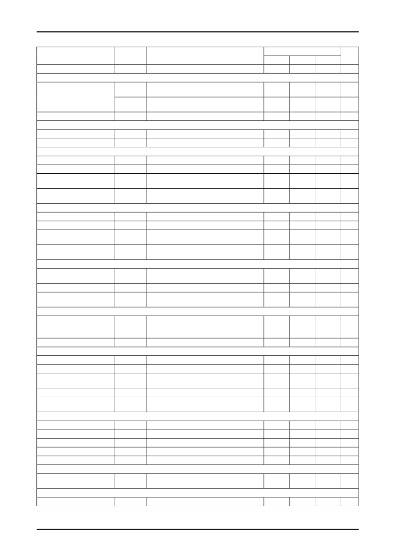
Electrical Characteristics
at Ta = 25
°
C, VCC = 5V, VS = 15V
Ratings
Parameter
Symbol
Conditions
min
typ
max
Unit
VCC supply current
Output
ICC
RL =
∞
, VCTL = 0, VLIM = 0V (Quiescent)
12
18
mA
VOsat1
IO = 500mA, Rf = 0.5
, sink+source
VCTL = VLIM = 5V (With saturation prevention)
IO = 1.0A, Rf = 0.5
, sink+source
VCTL = VLIM = 5V (With saturation prevention)
2.1
2.6
V
Output saturation voltage
VOsat2
2.6
3.5
V
Output leakage current
IOleak
1.0
mA
FR
FR pin input threshold voltage
VFSR
1.0
1.25
2
V
FR pin input input bias current
Ib (FSR)
VFR = 3V
100
150
200
μ
A
Control
CTL pin input Input bias current
Ib (CTL)
VCTL = 5V
1.5
3
μ
A
CTL pin input motor current
Imctl
VCTL = 0V
5
mA
CTL pin control start voltage
VCTL (ST)
Rf = 0.5
, VLIM = 5V, IO
≥
10mA
Hall input logic fixed (U, V, W = H, H, L)
Rf = 0.5
,
IO = 200mA
Hall input logic fixed (U, V, W = H, H, L)
2.25
2.50
2.75
V
CTL pin control Gm
Gm (CTL)
0.86
1.06
1.26
A/V
Current limit
LIM pin input current
Ilim
VLIM = 3V
1.5
3
μ
A
LIM pin motor current
Imlim
VLIM = 0V
5
mA
LIM current limit offset voltage
Voff (LIM)
Rf = 0.5
, VCTL = 5V, IO
≥
10mA
Hall input logic fixed (U, V, W = H, H, L)
Rf = 0.5
, VCTL = 5V
Hall input logic fixed (U, V, W = H, H, L)
1.0
1.25
1.5
V
LIM pin control Gm
Gm (lim)
0.59
0.71
0.83
A/V
Hall amplifier
Hall amplifier input offset voltage
VOFF
(HALL)
Ib (HALL)
-6
+6
mV
Hall amplifier input bias current
1.0
3.0
μ
A
Hall amplifier common-mode
input voltage
TRC
VCM (HALL)
1.3
3.3
V
Torque ripple correction ratio
TRC
For the high and low peaks in the Rf waveform when
IO = 200mA
(Rf = 0.5
, ADJ-OPEN) Note.2
13
%
ADJ pin voltage
VADJ
2.37
2.50
2.63
V
FG Amplifier
FG amplifier input offset voltage
VOFF (FG)
-8
+8
mV
FG amplifier input bias current
Ib (FG)
-100
nA
FG amplifier output saturation
voltage
FG amplifier voltage gain
VOsat (FG)
Sink side; With internal pull-up resistance load
0.5
0.6
V
VG (FG)
For open loop at f = 10kHz
41.5
44.5
47.5
dB
FG amplifier common-mode input
voltage
Schmitt amplifier
VCM (FG)
0.5
4.0
V
Duty ratio
DUTY
Under specified conditions (RF = 39k
) Note 3
49.0
50
51.0
%
Upper side output saturation voltage
Vsatu (SH)
IO = -20
μ
A
IO = 100
μ
A
4.8
V
Lower side output saturation voltage
Vsatd (SH)
0.2
V
Hysteresis width
Vhys
32
46
60
mV
FGS output pin pull-up resistance
RFGout
4.7
k
Saturation
Saturation prevention circuit
lower set voltage
TSD
VO sat
(DET)
Voltage between each OUT and Rf with
IO = 10mA, Rf = 0.5
, VCTL = VLIM = 5V
0.175
0.25
0.325
V
TSD operating temperature
Note 1. No measurements are made on the parameters with Note (Design target).
T-TSD
(Design target) Note.1
180
°
C
相關(guān)PDF資料 |
PDF描述 |
|---|---|
| LB11981 | Three-Phase Sensorless Motor Driver |
| LB11985 | VCR Capstan Motor Brushless Motor Driver |
| LB11985H | VCR Capstan Motor Brushless Motor Driver |
| LB11988 | Refrigerator Fan Motor Driver |
| LB11990W | Three-Phase Brushless Motor Driver |
相關(guān)代理商/技術(shù)參數(shù) |
參數(shù)描述 |
|---|---|
| LB11981 | 制造商:SANYO 制造商全稱:Sanyo Semicon Device 功能描述:Three-Phase Sensorless Motor Driver |
| LB11981-TLM-E | 制造商:Sony Semiconductor Solutions Division 功能描述: |
| LB11983 | 制造商:未知廠家 制造商全稱:未知廠家 功能描述: |
| LB11983-E | 功能描述:馬達(dá)/運(yùn)動(dòng)/點(diǎn)火控制器和驅(qū)動(dòng)器 FAN MOTOR RoHS:否 制造商:STMicroelectronics 產(chǎn)品:Stepper Motor Controllers / Drivers 類型:2 Phase Stepper Motor Driver 工作電源電壓:8 V to 45 V 電源電流:0.5 mA 工作溫度:- 25 C to + 125 C 安裝風(fēng)格:SMD/SMT 封裝 / 箱體:HTSSOP-28 封裝:Tube |
| LB11985 | 制造商:SANYO 制造商全稱:Sanyo Semicon Device 功能描述:VCR Capstan Motor Brushless Motor Driver |
發(fā)布緊急采購,3分鐘左右您將得到回復(fù)。