- 您現(xiàn)在的位置:買(mǎi)賣(mài)IC網(wǎng) > PDF目錄30725 > LA7577N FM, AUDIO SINGLE CHIP RECEIVER, PDIP24 PDF資料下載
參數(shù)資料
| 型號(hào): | LA7577N |
| 元件分類(lèi): | 接收器 |
| 英文描述: | FM, AUDIO SINGLE CHIP RECEIVER, PDIP24 |
| 封裝: | DIP-24 |
| 文件頁(yè)數(shù): | 5/16頁(yè) |
| 文件大小: | 354K |
| 代理商: | LA7577N |
第1頁(yè)第2頁(yè)第3頁(yè)第4頁(yè)當(dāng)前第5頁(yè)第6頁(yè)第7頁(yè)第8頁(yè)第9頁(yè)第10頁(yè)第11頁(yè)第12頁(yè)第13頁(yè)第14頁(yè)第15頁(yè)第16頁(yè)

LA7577N
No. 4037—13/16
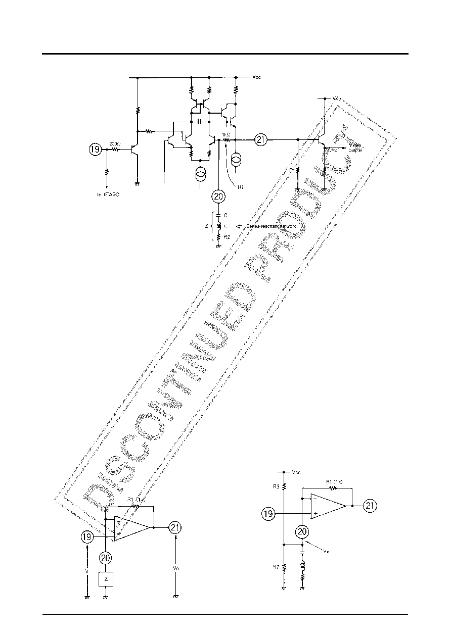
Equalization Amplier (Pins 19 to 21)
The video signal, after passing through the 4.5MHz trap, is
input on pin 19 to the equalization amplier, and output on
pin 21. A resistor should be connected between the emit-
ter-follower output and ground to ensure adequate output
drive capability. The resistor should be
≥2.7kΩ (V
CC =
12V) or
≥2.2kΩ (V
CC = 9V). A buffer transistor should be
used if the signal is taken off-board.
Equalization amplier design
The equalization amplier has an external series resonant
circuit, shown in Figure 24, which controls the frequency
characteristic. The output voltage, Vo, is given by the fol-
lowing equation:
Vo = (R1/Z + 1) (Vi + Vin)
Since the input voltage, Vin, is small, the gain is given
approximately by the following equation:
AV = Vo/Vi = R1/Z + 1
The amplier can be used as a voltage amplier by con-
necting a network to pin 20 as shown in Figure 25. The
bleeder resistor should be chosen to avoid excessive gain
and extreme video sync tip voltages.
Figure 24. Equalization amplier
Figure 25. Voltage amplier conguration
External bleeder resistor selection
If the equalization amplier is congured for non-unity
gain, bleeder resistors R2 and R3, shown in Figure 26, are
required to ensure that the output DC voltage does not
change.
The sync tip voltage does not change if VX is approxi-
mately equal to V21. VX is given by the following equa-
tion:
VX = VCC × R2/(R2 + R3)
The voltage gain is given by:
AV = 1 + 1000/Z1
where
Z1 = R2
× R3/(R2 + R3)
and resistors R2 and R3 are given by:
R2 = 1000
× V
CC/[(VCC VX) × (AV 1)]
R3 = 1000
× V
CC/[VX × (AV 1)]
Figure 26. External bleeder resistor circuit
相關(guān)PDF資料 |
PDF描述 |
|---|---|
| LA7577 | SPECIALTY CONSUMER CIRCUIT, PDIP24 |
| LA7578N | FM, AUDIO/VIDEO DEMODULATOR, PDIP24 |
| LA7583 | AUDIO/VIDEO DEMODULATOR, PDIP24 |
| LA7605M | SPECIALTY CONSUMER CIRCUIT, PQFP80 |
| LA76070 | SPECIALTY CONSUMER CIRCUIT, PDIP52 |
相關(guān)代理商/技術(shù)參數(shù) |
參數(shù)描述 |
|---|---|
| LA7578 | 制造商:未知廠(chǎng)家 制造商全稱(chēng):未知廠(chǎng)家 功能描述: |
| LA7578N | 制造商:SANYO 制造商全稱(chēng):Sanyo Semicon Device 功能描述:IF Signal Processing (Super PLL-II VIF + SIF) Circuit for TVs and VCRs |
| LA7583 | 制造商:SANYO 制造商全稱(chēng):Sanyo Semicon Device 功能描述:IF Signal Processing Circuit (A2C PLL VIF + SIF) for TVs and VCRs |
| LA7590 | 制造商:未知廠(chǎng)家 制造商全稱(chēng):未知廠(chǎng)家 功能描述:Analog IC |
| LA7600 | 制造商:未知廠(chǎng)家 制造商全稱(chēng):未知廠(chǎng)家 功能描述: |
發(fā)布緊急采購(gòu),3分鐘左右您將得到回復(fù)。