- 您現(xiàn)在的位置:買賣IC網(wǎng) > PDF目錄358734 > LA7138M (Sanyo Electric Co.,Ltd.) Monolithic Linear IC For the DVD Player Analog Video Signal I/F Driver PDF資料下載
參數(shù)資料
| 型號(hào): | LA7138M |
| 廠商: | Sanyo Electric Co.,Ltd. |
| 英文描述: | Monolithic Linear IC For the DVD Player Analog Video Signal I/F Driver |
| 中文描述: | 單片線性集成電路的DVD播放機(jī)模擬視頻信號(hào)I /女驅(qū)動(dòng) |
| 文件頁(yè)數(shù): | 2/13頁(yè) |
| 文件大?。?/td> | 332K |
| 代理商: | LA7138M |
第1頁(yè)當(dāng)前第2頁(yè)第3頁(yè)第4頁(yè)第5頁(yè)第6頁(yè)第7頁(yè)第8頁(yè)第9頁(yè)第10頁(yè)第11頁(yè)第12頁(yè)第13頁(yè)

LA7138M
No.A0220-2/16
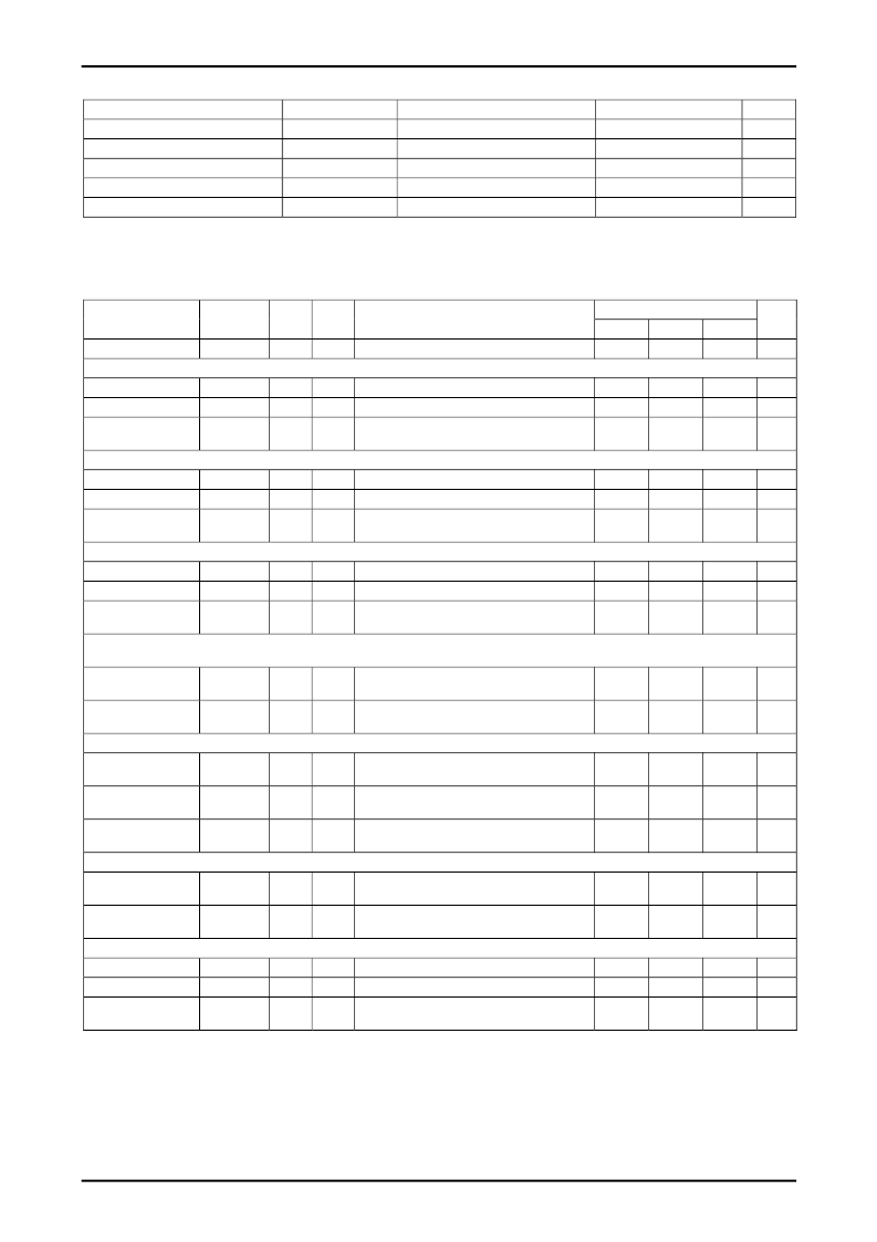
Recommended Operating Conditions
at Ta = 25
°
C
Parameter
Symbol
Conditions
Ratings
Unit
Recommended supply voltage A
VCC A
VCCop A
VCC B
VCCop B
VIN
*
12.0
V
Operating supply voltage range A
9.0 to 13.0
V
Recommended supply voltage B
*
8.0
V
Operating supply voltage range B
7.5 to 8.5
V
Input pin voltage application range
VCCop A, B+0.3
≤
13V
-0.3 to VCCop A, B+0.3
V
*:A different operation circuit is recommended for recommended supply voltages A and B. An external operation circuit with a PNP transistor for voltage drop is
recommended for the recommended supply voltage A.
Electrical Characteristics
at Ta = 25
°
C, VCCA = 9.0 to 13.0V,VCCB = 7.5 to 8.5V
Ratings
Parameter
Symbol
Input
signal
Test
point
Conditions
min
typ
max
Unit
Current drain (1)
ICC1
9pin
Current drain of VIDEO system.
29.6
37.0
44.4
mA
(A) Pin 10 (Y signal) input when the composite/S is selected.
AMP-GAIN (Low)
GYM
GYH
C10H
Sig.1
T13/15
GAIN when 996mVp-p, 100kHz is entered.
5.05
5.27
5.48
dB
AMP-GAIN (High)
Sig.1
T13/15
GAIN when 761mVp-p, 100kHz is entered.
7.38
7.6
7.81
dB
Clamp voltage
Sig.1
T10
Potential of sink chip of T10 when 761mVp-p is
entered.
3.85
4.20
4.55
V
(B) Pin 6 (chroma signal) input when the composite/S is selected.
AMP-GAIN (Low)
GCM
GCH
Sig.2
T17/19
GAIN when 711mVp-p, 3.58MHz is entered.
5.05
5.27
5.48
dB
AMP-GAIN (High)
Sig.2
T17/19
GAIN when 544mVp-p, 3.58MHz is entered.
7.38
7.6
7.81
dB
Chroma input
DC voltage
(C) Pin 3 (composite signal) input when the composite is selected.
D6H
Sig.2
T6
Offset voltage of T6 when 544 mVp-p is entered.
4.4
4.75
5.1
V
AMP-GAIN (Low)
GSM1
GSH1
C3H
Sig.3
T21/23
GAIN when 996mVp-p, 100kHz is entered.
5.05
5.27
5.48
dB
AMP-GAIN (High)
Sig.3
T21/23
GAIN when 761mVp-p, 100kHz is entered.
7.38
7.6
7.81
dB
Clamp voltage
Sig.3
T3
Potential of sink chip of T3 when 761mVp-p is
entered.
4.0
4.35
4.7
V
(D) Pins 6, 10 (S signal) input when the S is selected.
To select “S”, insert a 5.1k
resistor in series with pin 2, (See the block diagram.)
AMP-GAIN (Low)
GSM2
Sig.1
Sig.2
AMP-GAIN (High)
GSH2
Sig.1
Sig.2
(E) GAIN ratio of signals when the composite is selected.
T21/23
GAIN when 996mVp-p, 100kHz or 711mVp-p,
3.58MHz is entered.
GAIN when 761mVp-p, 100kHz or 544mVp-p,
3.58MHz is entered.
4.92
5.27
5.61
dB
T21/23
7.25
7.6
7.94
dB
Y/chroma
-AMP-GAIN ratio
Y/composite-AMP-
GAIN ratio
Chroma/composite
-AMP-GAIN ratio
(F) GAIN ratio of signals when the S signal is selected.
YC
Sig.1
Sig.2
Sig.1
Sig.3
Sig.2
Sig.3
T13/15T
17/19
T13/15
T21/23
T17/19
T21/23
GAIN ratio between GYH of (A) and GCH of (B).
-3
0
3
%
YS1
GAIN ratio between GYH of (A) and GSH1 of (C).
-3
0
3
%
CS1
GAIN ratio between GCH of (B) and GSH1 of (C).
-3
0
3
%
Y/S-AMP-GAIN ratio
YS2
Sig.1
Sig.2
Sig.1
Sig.2
T13/15
T21/23
T17/19
T21/23
GAIN ratio between GYH of (A) and GSH2 of (D)
-4.5
0
4.5
%
Chroma/S-AMP-
GAIN ratio
(G) Pin 10 (Y signal) input when the component is selected.
CS2
GAIN ratio between GCH of (B) and GSH2 of (D).
-4.5
0
4.5
%
AMP-GAIN (Low)
GYM
GYH
C10H
Sig.1
T13/15
GAIN when 996mVp-p, 100 kHz is entered.
5.05
5.27
5.48
dB
AMP-GAIN (High)
Sig.1
T13/15
GAIN when 761mVp-p, 100 kHz is entered.
7.38
7.6
7.81
dB
Y input clamp voltage
Sig.1
T10
Potential of sink chip of T10 when 761mVp-p is
entered.
3.85
4.20
4.55
V
Continued on next page.
相關(guān)PDF資料 |
PDF描述 |
|---|---|
| LA7150 | Audio/Video Switch for PAL System VCR |
| LA7151 | Audio/Video Switch for VCR Video Camera Use |
| LA7151M | Audio/Video Switch for VCR Video Camera Use |
| LA71525M | Video/audio signal processor for VHS VCRs |
| LA7152 | VCR Electronic Switch |
相關(guān)代理商/技術(shù)參數(shù) |
參數(shù)描述 |
|---|---|
| LA7140 | 制造商:未知廠家 制造商全稱:未知廠家 功能描述: |
| LA7150 | 制造商:SANYO 制造商全稱:Sanyo Semicon Device 功能描述:Audio/Video Switch for PAL System VCR |
| LA7151 | 制造商:SANYO 制造商全稱:Sanyo Semicon Device 功能描述:Audio/Video Switch for VCR Video Camera Use |
| LA7151M | 制造商:SANYO 制造商全稱:Sanyo Semicon Device 功能描述:Audio/Video Switch for VCR Video Camera Use |
| LA7152 | 制造商:SANYO 制造商全稱:Sanyo Semicon Device 功能描述:VCR Electronic Switch |
發(fā)布緊急采購(gòu),3分鐘左右您將得到回復(fù)。