- 您現(xiàn)在的位置:買賣IC網(wǎng) > PDF目錄32287 > LA3361 FM, AUDIO DEMODULATOR, PDIP16 PDF資料下載
參數(shù)資料
| 型號: | LA3361 |
| 元件分類: | 接收器 |
| 英文描述: | FM, AUDIO DEMODULATOR, PDIP16 |
| 封裝: | DIP-16 |
| 文件頁數(shù): | 7/8頁 |
| 文件大?。?/td> | 365K |
| 代理商: | LA3361 |

LA3361
No.505–7/8
Proper cares in using the IC
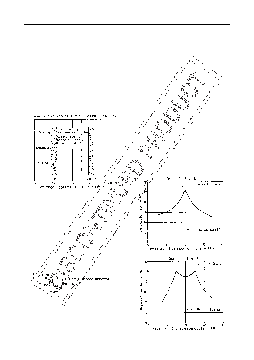
(1) Pin 9-used control
Pin 9 is for stereo/monaural selection and VCO stop.
When a voltage of less than 0.7V is applied to pin 9 or
pin 9 is grounded or brought into the open state, the
stereo (automatic) mode is entered. When a voltage of
more than 2.1V is applied to pin 9, the VCO stops oper-
ating and the stereo indicator is prevented from mal-
functioning. Therefore, no external measure against
malfunction is required. When applying a voltage to pin
9, the following should be noted. An applied voltage of
approximately 0.7V or 2.1V causes the internal transis-
tors to enter the active region and hum or noise is liable
to enter pin 9. Therefore, for example, the applied volt-
age must be set to an intermediate voltage such as 0V,
1.4V, 2.8V.
When the VCO stop mode caused by application of a
voltage to pin 9 is released, the stereo indicator may be
turned ON momentarily. This phenomenon is liable to
occur if the value of the capacitor across pins 10 and 11
is large (C10-11>2 to 3μF). The reason for this is that if
the VCO stop mode and forced monaural mode are re-
leased simultaneously when the C10-11 is charged with
the pin 10 side being at “H” level at the VCO stop mode,
the trigger circuit is turned ON until the C10-11 is dis-
charged. This can be prevented by making the release
of the forced monuarl mode a little later than that of the
VCO stop mode. For this purpose, the C9 is connected
across pin 9 and GND as shown below so that the volt-
age on pin 9 drops slowly at the time of release.
C9>2C10-11 is a rule-of thumb guide for the relation
between C9 and C10-11 which prevents the stereo in-
dicator from being turned ON mistakenly.
(2) Loop filter capacitor C14-15
When your set is designed with an input signal level of
250mV or greater, the C14-15 is 1μF. The capture range
tends to extend with the input level. When your set is
designed with a high input signal level of 250mV or
greater, your set is liable to be affected by high-fre-
quency signals or noises. Therfore, the loop filter ca-
pacitor (across pins 14 and 15) should be made large to
narrow the filter bandwidth. If C14-15=1μF is used in
your set with an input signal level of 250mV or greater,
the capture range is made a little narrower and your set
is hard to be affected by high-frequency signals.
(3) Phase compensation capactor (See Fig. 8)
A capacitor of 620pF is connected across pin 3 and GND
to compensate the phase lead caused by the decoupling
capacitor across pins 3 and 13 and the phase shift caused
by the PLL. If no phase compensation capacitor is con-
nected, the center of the separation characteristic plot-
ted against the free-running frequency is off 19.00kHz
and the margin for the free-running frequency drift and
adjustment error becomes narrow. Therefore, phase
compensation should be done.
(4) Separation control
The separation control is done to provide a single or
double hump response in the separation vs. free-run-
ning frequency characteristic as shown on next page.
相關(guān)PDF資料 |
PDF描述 |
|---|---|
| LA3600 | 1 CHANNEL(S), EQUALIZER CIRCUIT, PDIP16 |
| LA3607 | 1 CHANNEL(S), EQUALIZER CIRCUIT, PDIP20 |
| LA4146 | 0.9 W, 1 CHANNEL, AUDIO AMPLIFIER, PSIP9 |
| LA42031 | 5 W, 1 CHANNEL, AUDIO AMPLIFIER, SFM13 |
| LA42031 | 5 W, 1 CHANNEL, AUDIO AMPLIFIER, SFM13 |
相關(guān)代理商/技術(shù)參數(shù) |
參數(shù)描述 |
|---|---|
| LA3365 | 制造商:SANYO 制造商全稱:Sanyo Semicon Device 功能描述:PLL MULTIPLEX STEREO DEMODULATOR |
| LA3366 | 制造商:未知廠家 制造商全稱:未知廠家 功能描述:Hyper 3mm (T1) LED/Diffused Hyper-Bright LED |
| LA3366-PS | 制造商:INFINEON 制造商全稱:Infineon Technologies AG 功能描述:Hyper 3 mm T1 LED, Diffused Hyper-Bright LED |
| LA3366-Q | 制造商:INFINEON 制造商全稱:Infineon Technologies AG 功能描述:Hyper 3 mm T1 LED, Diffused Hyper-Bright LED |
| LA3366-QT | 制造商:INFINEON 制造商全稱:Infineon Technologies AG 功能描述:Hyper 3 mm T1 LED, Diffused Hyper-Bright LED |
發(fā)布緊急采購,3分鐘左右您將得到回復。