- 您現(xiàn)在的位置:買賣IC網(wǎng) > PDF目錄367493 > L8560 Low-Power SLIC with Ringing PDF資料下載
參數(shù)資料
| 型號(hào): | L8560 |
| 英文描述: | Low-Power SLIC with Ringing |
| 中文描述: | 低功耗振鈴用戶接口 |
| 文件頁數(shù): | 29/46頁 |
| 文件大?。?/td> | 842K |
| 代理商: | L8560 |
第1頁第2頁第3頁第4頁第5頁第6頁第7頁第8頁第9頁第10頁第11頁第12頁第13頁第14頁第15頁第16頁第17頁第18頁第19頁第20頁第21頁第22頁第23頁第24頁第25頁第26頁第27頁第28頁當(dāng)前第29頁第30頁第31頁第32頁第33頁第34頁第35頁第36頁第37頁第38頁第39頁第40頁第41頁第42頁第43頁第44頁第45頁第46頁

Lucent Technologies Inc.
29
Data Sheet
April 2000
L8560 Low-Power SLIC with Ringing
Applications
(continued)
Power Ringing
(continued)
Current-Limit Switch
During nonringing modes, the internal current source is
set at 75
μ
A. During the ring mode, the current limit is
automatically increased by a factor of 2.8. This is done
to provide sufficient ring to a true North American 5
REN load. This is done internally by increasing the
value of I
PROG
from 75
μ
A to 210
μ
A, thus:
I
PROG
R
PROG
= l
LIM
B
DCOUT
R
PROG
= l
LIM
B
DCOUT
/I
PROG
R
PROG
(K) = l
LIM
(mA)
0.04167 (V/mA)/210e–3 (mA)
R
PROG
(K) = 0.198
l
LIM
(mA)
In the current-limit region, the dc template has a high
resistance (12.5 k
).
Ring Trip
Ring trip is accomplished by filtering the voltage seen
at node DCOUT and applying it to the integrated ring
trip comparator. DCOUT is a voltage proportional to the
tip/ring current, and under short dc loop conditions, on-
hook ringing current and off-hook current provide suffi-
cient voltage differential at DCOUT to distinguish that a
ring trip condition has occurred. The ring trip compara-
tor threshold is set via a resistor between the ring trip
comparator and ground.
Output NSTAT is automatically set to detect ring trip
during the balanced ring mode. During quiet intervals
of ringing, output NSTAT is automatically determined
by the loop closure detector.
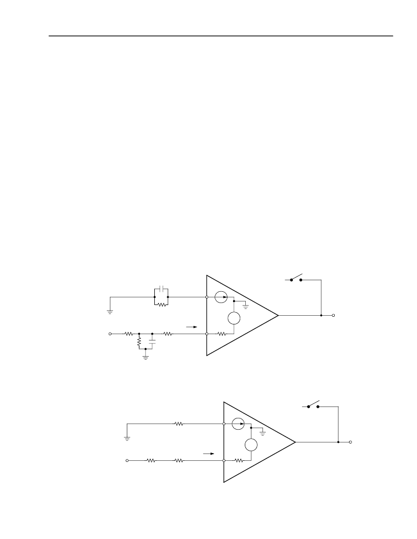
The equivalent ring trip circuit for the balanced ringing
SLIC application is shown in Figure 31.
The equations governing ring trip are derived below.
Capacitors C
2
and C
4
, in conjunction with resistors R
2
and R
4
, form a double-pole, low-pass filter that
smooths the voltage seen at DCOUT. The poles of the
filters are determined by C
2
and C
4
. Where these poles
are set will influence both the ripple seen at DCOUT
and the speed of the transition of the voltage at
DCOUT from the pretrip to the tripped level. For the
derivation of the ring trip threshold equations, capaci-
tors C
2
and C
4
can be ignored.
Redrawing the circuit, ignoring the capacitors, and tak-
ing the Thevenin equivalent circuit of the network at
RTSN gives the results shown below in Figure 32.
12-3349.b (F)
Figure 31. Equivalent Ring Trip Circuit for Balanced Ringing SLIC
12-3348.b (F)
Figure 32. Thevenin Equivalent Ring Trip Circuit for Balanced Ringing SLIC
–
+
15 k
8.2 V
I
P
= I
N
R
2
NRDET
R
TSP
I
N
R
TSN
NSTAT
NLC
R
4
R
1
DCOUT
C
2
R
3
C
4
–
+
15 k
8.2 V
I
P
= I
N
R
2
NRDET
R
TSP
I
N
R
TSN
NSTAT
NLC
R
4
R
1
R
3
/(R
1
+ R
3
)
(R
3
/[R
1
+ R
3
]) DCOUT
相關(guān)PDF資料 |
PDF描述 |
|---|---|
| L8567 | SLIC for Peoples Republic of China Applications |
| L8567-32PLCC | Telecommunication IC |
| L8567-44PLCC | Telecommunication IC |
| L8574D | CAP 15PF 50V 5% C0G SMD-0402 TR-7-PA SN100 |
| L8575 | Dual-Resistive,Low-Cost Subscriber Line Interface Circuit(SLIC) |
相關(guān)代理商/技術(shù)參數(shù) |
參數(shù)描述 |
|---|---|
| L8560AAU | 制造商:Alcatel-Lucent 功能描述: 制造商:LUCENT 功能描述: |
| L8561 | 制造商:UTC-IC 制造商全稱:UTC-IC 功能描述:The UTC L8561 is a Power Factor Corrector, which can work in wide input voltage range applications (from 85V ~ 265V) with an excellent THD. |
| L8561_11 | 制造商:UTC-IC 制造商全稱:UTC-IC 功能描述:POWER FACTOR CORRECTOR |
| L8561G-D08-T | 制造商:UTC-IC 制造商全稱:UTC-IC 功能描述:POWER FACTOR CORRECTOR |
| L8561G-S08-R | 制造商:UTC-IC 制造商全稱:UTC-IC 功能描述:POWER FACTOR CORRECTOR |
發(fā)布緊急采購,3分鐘左右您將得到回復(fù)。