- 您現(xiàn)在的位置:買賣IC網(wǎng) > PDF目錄383238 > L6910TR (意法半導體) ADJUSTABLE STEP DOWN CONTROLLER WITH SYNCHRONOUS RECTIFICATION PDF資料下載
參數(shù)資料
| 型號: | L6910TR |
| 廠商: | 意法半導體 |
| 英文描述: | ADJUSTABLE STEP DOWN CONTROLLER WITH SYNCHRONOUS RECTIFICATION |
| 中文描述: | 可調(diào)降壓控制器采用同步整流 |
| 文件頁數(shù): | 8/21頁 |
| 文件大?。?/td> | 453K |
| 代理商: | L6910TR |
L6910A L6910
8/21
Where
I is the inductance ripple current and I
OUTMAX
is the maximum output current.
In case of over current detectionthe soft start capacitor is discharged with constant current (10
μ
A typ.) and when
the SS pin reaches 0.5V the soft start phase is restarted. During the soft start the over-current protection is al-
ways active and if such kind of event occurs, the device turns off both mosfets, and the SS capacitor is dis-
charged again (after reaching the upper threshold of about 4V). The system is now working in HICCUP mode,
as shown in figure 5. After removing the cause of the over-current, the device restart working normally without
power supplies turn off and on.
I
P
I
OUTMAX
I
2
----
+
≥
I
PEAK
=
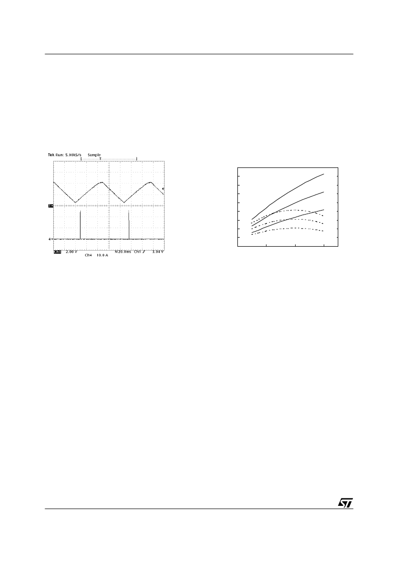
Figure 5. Hiccup Mode
Figure 6. Inductor ripple current vs. Vout
CH1 = SS; CH4 = Inductor current
0
1
2
3
4
5
6
7
8
9
0.5
1.5
2.5
3.5
Output Voltage [V]
I
L=3
μ
H,
Vin=12V
L=2
H,
Vin=12V
L=1.5
μ
H, Vin=12V
L=2
μ
H,
Vin=5V
L=1.5
μ
H,
Vin=5V
L=3
μ
H, Vin=5V
Inductor design
The inductance value is defined by a compromise between the transient response time, the efficiency, the cost
and the size. The inductor has to be calculated to sustain the output and the input voltage variation to maintain
the ripple current
I
L
between 20% and 30% of the maximum output current. The inductance value can be cal-
culated with this relationship:
V
V
–
f
sw
Where f
SW
is the switching frequency, V
IN
is the input voltage and V
OUT
is the output voltage. Figure 6 shows
the ripple current vs. the output voltage for different values of the inductor, with V
IN
= 5V and V
IN
= 12V.
Increasing the value of the inductance reduces the ripple current but, at the same time, reduces the converter
response time to a load transient. If the compensation network is well designed, the device is able to open or
close the duty cycle up to 100% or down to 0%. The response time is now the time required by the inductor to
change its current from initial to final value. Since the inductor has not finished its charging time, the output cur-
rent is supplied by the output capacitors. Minimizing the response time can minimize the output capacitance
required.
The response time to a load transient is different for the application or the removal of the load: if during the ap-
plication of the load the inductor is charged by a voltage equal to the difference between the input and the output
voltage, during the removal it is discharged only by the output voltage. The following expressions give approx-
imate response time for
I load transient in case of enough fast compensation network response:
V
IN
V
OUT
–
The worst condition depends on the input voltage available and the output voltage selected. Anyway the worst
case is the response time after removal of the load with the minimum output voltage programmed and the max-
imum input voltage available.
L
I
L
------------------------------
V
V
IN
--------------
=
t
application
------------------------------
t
removal
V
OUT
I
--------------
=
=
相關PDF資料 |
PDF描述 |
|---|---|
| L6911D | 5 BIT PROGRAMMABLE STEP DOWN CONTROLLER WITH SYNCHRONOUS RECTIFICATION |
| L6911DTR | 5 BIT PROGRAMMABLE STEP DOWN CONTROLLER WITH SYNCHRONOUS RECTIFICATION |
| L6918 | 5 BIT PROGRAMMABLE MULTIPHASE CONTROLLER |
| L6918A | 5 BIT PROGRAMMABLE MULTIPHASE CONTROLLER |
| L6918AD | 5 BIT PROGRAMMABLE MULTIPHASE CONTROLLER |
相關代理商/技術參數(shù) |
參數(shù)描述 |
|---|---|
| L6911 | 制造商:STMICROELECTRONICS 制造商全稱:STMicroelectronics 功能描述:5 BIT PROGRAMMABLE POWER SUPPLY CONTROLLER FOR PENTIUM II PROCESSOR |
| L6911A | 制造商:未知廠家 制造商全稱:未知廠家 功能描述:Industrial Control IC |
| L6911B | 制造商:STMicroelectronics 功能描述: |
| L6911C | 功能描述:DC/DC 開關控制器 5B PROGRAMMABLE STEP DOWN CONTROLLER RoHS:否 制造商:Texas Instruments 輸入電壓:6 V to 100 V 開關頻率: 輸出電壓:1.215 V to 80 V 輸出電流:3.5 A 輸出端數(shù)量:1 最大工作溫度:+ 125 C 安裝風格: 封裝 / 箱體:CPAK |
| L6911CTR | 功能描述:DC/DC 開關控制器 5B PROGRAMMABLE STEP DOWN CONTROLLER RoHS:否 制造商:Texas Instruments 輸入電壓:6 V to 100 V 開關頻率: 輸出電壓:1.215 V to 80 V 輸出電流:3.5 A 輸出端數(shù)量:1 最大工作溫度:+ 125 C 安裝風格: 封裝 / 箱體:CPAK |
發(fā)布緊急采購,3分鐘左右您將得到回復。