- 您現(xiàn)在的位置:買賣IC網(wǎng) > PDF目錄383234 > L5970AD (意法半導(dǎo)體) RADIATION HARDENED HIGH EFFICIENCY, 5 AMP SWITCHING REGULATORS PDF資料下載
參數(shù)資料
| 型號: | L5970AD |
| 廠商: | 意法半導(dǎo)體 |
| 元件分類: | 基準(zhǔn)電壓源/電流源 |
| 英文描述: | RADIATION HARDENED HIGH EFFICIENCY, 5 AMP SWITCHING REGULATORS |
| 中文描述: | 抗輻射高效,5安培開關(guān)穩(wěn)壓器 |
| 文件頁數(shù): | 6/11頁 |
| 文件大小: | 135K |
| 代理商: | L5970AD |
L5970AD
6/11
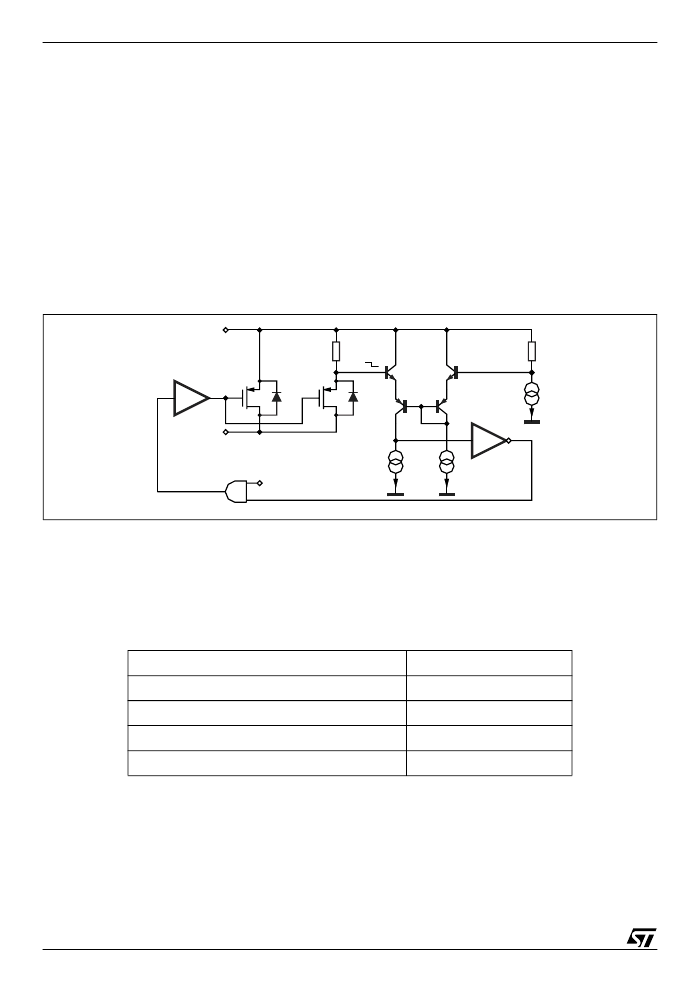
3.4 CURRENT PROTECTION
The L5970AD has two current limit protections, pulse by pulse and frequency fold back.
The schematic of the current limitation circuitry for the pulse by pulse protection is shown in figure 7.
The output power PDMOS transistor is split in two parallel PDMOS. The smallest one has a resistor in series,
R
SENSE
. The current is sensed through Rsense and if reaches the threshold, the mirror is unbalanced and the
PDMOS is switched off until the next falling edge of the internal clock pulse.
Due to this reduction of the ON time, the output voltage decreases.
Since the minimum switch ON time (necessary to avoid false overcurrent signal) is not enough to obtain a suf-
ficiently low duty cycle at 500KHz, the output current, in strong overcurrent or short circuit conditions, could in-
crease again. For this reason the switching frequency is also reduced, so keeping the inductor current under its
maximum threshold. The Frequency Shifter (see fig. 6) depends on the feedback voltage. As the feedback volt-
age decreases (due to the reduced duty cycle), the switching frequency decreases too.
Figure 7. Current Limitation Circuitry
3.5 ERROR AMPLIFIER
The voltage error amplifier is the core of the loop regulation. It is a transconductance operational amplifier whose
non inverting input is connected to the internal voltage reference (1.235V), while the inverting input (FB) is con-
nected to the external divider or directly to the output voltage. The output (COMP) is connected to the external
compensation network.
The uncompensated error amplifier has the following characteristics:
The error amplifier output is compared with the oscillator sawtooth to perform PWM control.
3.6 PWM COMPARATOR AND POWER STAGE
This block compares the oscillator sawtooth and the error amplifier output signals generating the PWM
signal for the driving stage.
The power stage is a very critical block cause it has to guarantee a correct turn on and turn off of the PD-
MOS.
Transconductance
2300
μ
S
Low frequency gain
65dB
Minimum sink/source voltage
1500
μ
A/300
μ
A
Output voltage swing
0.4V/3.65V
Input bias current
2.5
μ
A
DRIVER
NOT
A1
PWM
VCC
OUT
A1/A2=95
I
L
RSENSE
D00IN1134
I
OFF
I
I
RTH
A2
相關(guān)PDF資料 |
PDF描述 |
|---|---|
| L5970ADTR | RADIATION HARDENED HIGH EFFICIENCY, 5 AMP SWITCHING REGULATORS |
| L5970D013 | RADIATION HARDENED HIGH EFFICIENCY, 5 AMP SWITCHING REGULATORS |
| L5970 | RADIATION HARDENED HIGH EFFICIENCY, 5 AMP SWITCHING REGULATORS |
| L5970D | RADIATION HARDENED HIGH EFFICIENCY, 5 AMP SWITCHING REGULATORS |
| L5970D013TR | RADIATION HARDENED HIGH EFFICIENCY, 5 AMP SWITCHING REGULATORS |
相關(guān)代理商/技術(shù)參數(shù) |
參數(shù)描述 |
|---|---|
| L5970ADTR | 功能描述:直流/直流開關(guān)調(diào)節(jié)器 STEP DOWN MONOLITHIC SWITCH REG 1.5A RoHS:否 制造商:International Rectifier 最大輸入電壓:21 V 開關(guān)頻率:1.5 MHz 輸出電壓:0.5 V to 0.86 V 輸出電流:4 A 輸出端數(shù)量: 最大工作溫度: 安裝風(fēng)格:SMD/SMT 封裝 / 箱體:PQFN 4 x 5 |
| L5970D | 功能描述:直流/直流開關(guān)調(diào)節(jié)器 1.2 to 35V Step-Down RoHS:否 制造商:International Rectifier 最大輸入電壓:21 V 開關(guān)頻率:1.5 MHz 輸出電壓:0.5 V to 0.86 V 輸出電流:4 A 輸出端數(shù)量: 最大工作溫度: 安裝風(fēng)格:SMD/SMT 封裝 / 箱體:PQFN 4 x 5 |
| L5970D_07 | 制造商:STMICROELECTRONICS 制造商全稱:STMicroelectronics 功能描述:Up to 1A step down switching regulator |
| L5970D_0710 | 制造商:STMICROELECTRONICS 制造商全稱:STMicroelectronics 功能描述:Up to 1A step down switching regulator |
| L5970D013 | 制造商:STMICROELECTRONICS 制造商全稱:STMicroelectronics 功能描述:UP TO 1A STEP DOWN SWITCHING REGULATOR |
發(fā)布緊急采購,3分鐘左右您將得到回復(fù)。