- 您現(xiàn)在的位置:買賣IC網(wǎng) > PDF目錄383234 > L4990 (意法半導(dǎo)體) PRIMARY CONTROLLER PDF資料下載
參數(shù)資料
| 型號: | L4990 |
| 廠商: | 意法半導(dǎo)體 |
| 英文描述: | PRIMARY CONTROLLER |
| 中文描述: | 主控制器 |
| 文件頁數(shù): | 15/24頁 |
| 文件大小: | 322K |
| 代理商: | L4990 |
ing conditionsrange, in terms of input voltageand
output current, that the converter is able to cover
but, on the other hand, the higher is the peak cur-
rent on the secondaryside.
As to this point, the L4990 turns out to be particu-
larly useful since it allows to set any maximum
duty cycle greater (and lower) than 50% with very
good precision. In the present case, a maximum
duty cycle of 60% for steady state operation has
been selected and an extra 5% is allowed to take
transients into account.
Since it is not requested a very tight tolerance on
the output, the feedback employs a primary side
voltage sensing technique to reduce cost and
complexity of the circuit. The same technique has
been used to protectagainst outputovervoltages.
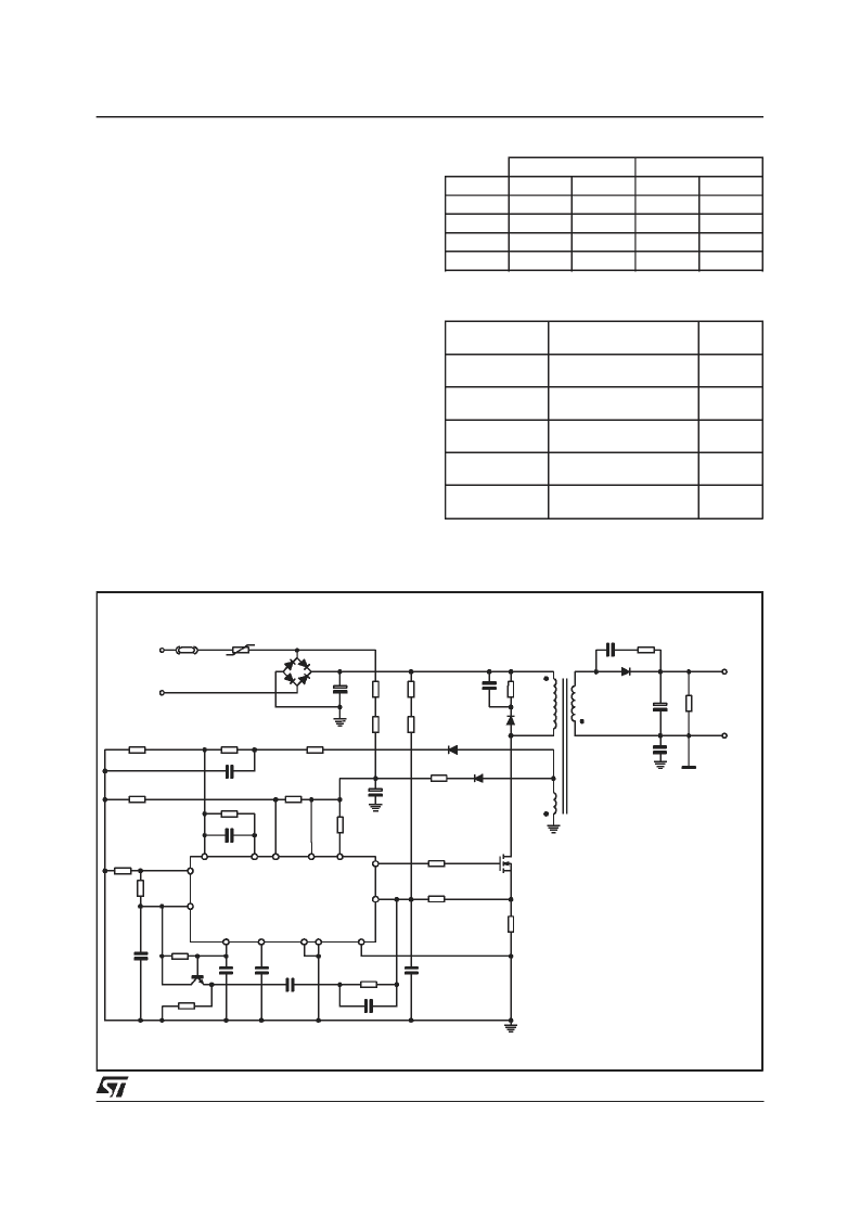
The electric schematic is shown in fig. 30. The
PCB layout is shown in figg. 31 and 32. Table 1
and 2 summarize typical system performance,
while table 3 lists the relevant bill of material,
where details are given only for critical compo-
nents and/orwhere useful.
Warning:
the NTC for inrush current limitation is
not assembled,thus use cautionwhen connecting
the demo board to the mains directly. The use of
a variac or an isolation transformer is recom-
mended.
Table 1. Systemefficiency.
I
out
= 1A
I
out
= 2A
V
in
(Vac)
85
110
220
270
V
out
(V)
14.93
14.95
14.95
14.96
Effic. %
83.7
82.5
81.4
76
V
out
(V)
14.53
14.55
14.57
14.59
Effic. %
84.3
84.9
85.2
81.6
Table 2. Systemperformance.
Line regulation
V
in
= 85 to 270 Vac
I
out
= 0.5A
V
in
= 85 Vac
V
in
= 270 Vac
V
in
= 190 Vac
I
out
= 2A
V
in
= 85 to 270 Vac
I
out
= 2A
V
in
= 270 Vac
V
out
< 20V
From C.C.M to D.C.M
I
out
= 2A
30mV
Load regulation
I
out
= 0.5A to 2A
Maximum effic.
0.95V
0.90V
86.2%
Output ripple
< 200mV
Minimum load
150mA
Transition Volt.
160V
85
to
270
Vac
B1
C1
R12
R19
C8
NTC
10
R7
13
R24
15
12
R11
8
14
6
R6
R15
R2
4
3
2
R9
C4
R10
7
R23
Q1
R16
C12
D3
D4
C2
R17
GND
D97IN499B
L4990
R13
R1
C10
C13
D2
R14
R5
C3
R3
C7
R4
5
9
DCC
R8
VREF
C5
C6
Q2
RCT
SS
R22
C15
DC-LIM
SGND
C14
R20
R21
C11
11
PGND
ISEN
OUT
VC
VCC
DIS
COMP
VFB
T1
15V/2A
D1
Figure 30. AC-DC adaptorelectric schematic
L4990 - L4990A
15/24
相關(guān)PDF資料 |
PDF描述 |
|---|---|
| L4990A | PRIMARY CONTROLLER |
| L4990AD | PRIMARY CONTROLLER |
| L4990D | PRIMARY CONTROLLER |
| L4992 | TRIPLE OUTPUT POWER SUPPLY CONTROLLER |
| L5170 | CAP CER 47000PF 50V X7R 0805 |
相關(guān)代理商/技術(shù)參數(shù) |
參數(shù)描述 |
|---|---|
| L4990A | 制造商:STMICROELECTRONICS 制造商全稱:STMicroelectronics 功能描述:PRIMARY CONTROLLER |
| L4990AD | 制造商:STMICROELECTRONICS 制造商全稱:STMicroelectronics 功能描述:PRIMARY CONTROLLER |
| L4990D | 制造商:STMICROELECTRONICS 制造商全稱:STMicroelectronics 功能描述:PRIMARY CONTROLLER |
| L4991 | 功能描述:TEST COIL FOR REED SWITCH, 1PC RoHS:是 類別:開關(guān) >> 配件 系列:- 標(biāo)準(zhǔn)包裝:100 系列:- 其它名稱:886.0007886.0007-ND |
| L4992 | 制造商:STMicroelectronics 功能描述: 制造商:STMicroelectronics 功能描述:VOLT SUPERVISOR CNTRLR 5.1V/3.3V 32TQFP - Trays |
發(fā)布緊急采購,3分鐘左右您將得到回復(fù)。