- 您現(xiàn)在的位置:買賣IC網(wǎng) > PDF目錄383231 > L4915 (意法半導(dǎo)體) ADJUSTABLE VOLTAGE REGULATOR PLUS FILTER PDF資料下載
參數(shù)資料
| 型號(hào): | L4915 |
| 廠商: | 意法半導(dǎo)體 |
| 英文描述: | ADJUSTABLE VOLTAGE REGULATOR PLUS FILTER |
| 中文描述: | 可調(diào)穩(wěn)壓器和過(guò)濾器 |
| 文件頁(yè)數(shù): | 3/7頁(yè) |
| 文件大?。?/td> | 99K |
| 代理商: | L4915 |
ELECTRICALCHARACTERISTICS
(continued)
(T
amb
= 25
o
C; V
i
= 13.5 V, V
O
= 8.5V,circuit of Fig. 1, unlessotherwise specified)
Symbol
V
O
T
SVR
Parameter
Test Conditions
Min.
Typ.
Max.
Unit
Output Voltage Drift
I
o
= 10mA
1.2
mV/
°
C
Supply Voltage Rejection
V
iac
= 1V
, f = 100Hz, I
o
= 150mA
Regulator
Filter Mode
71
35(*)
300
dB
I
SC
T
on
Short Circuit Current
Switch On Time
250
mA
ms
I
o
= 150mA
Regulator
Filter Mode
300
500(*)
145
T
j
Thermal Shutdown Junction
Temperature
°
C
(*) Depending of the C
FT
capacitor
PRINCIPLE OF OPERATION
Duringnormal operation(input voltageupper than
V
I MIN
= V
OUT NOM
+
V
I/O
). The deviceworks as a
normal voltage regulator built around the OP1 of
the blockdiagram.
TheseriespasselementusesaPNP-NPN connec-
tion to reduce the dropout. The reference voltage
of theOP1 is derivedfrom a REF through the OP2
and Q3, acting as an active zener diode of value
V
REF
.
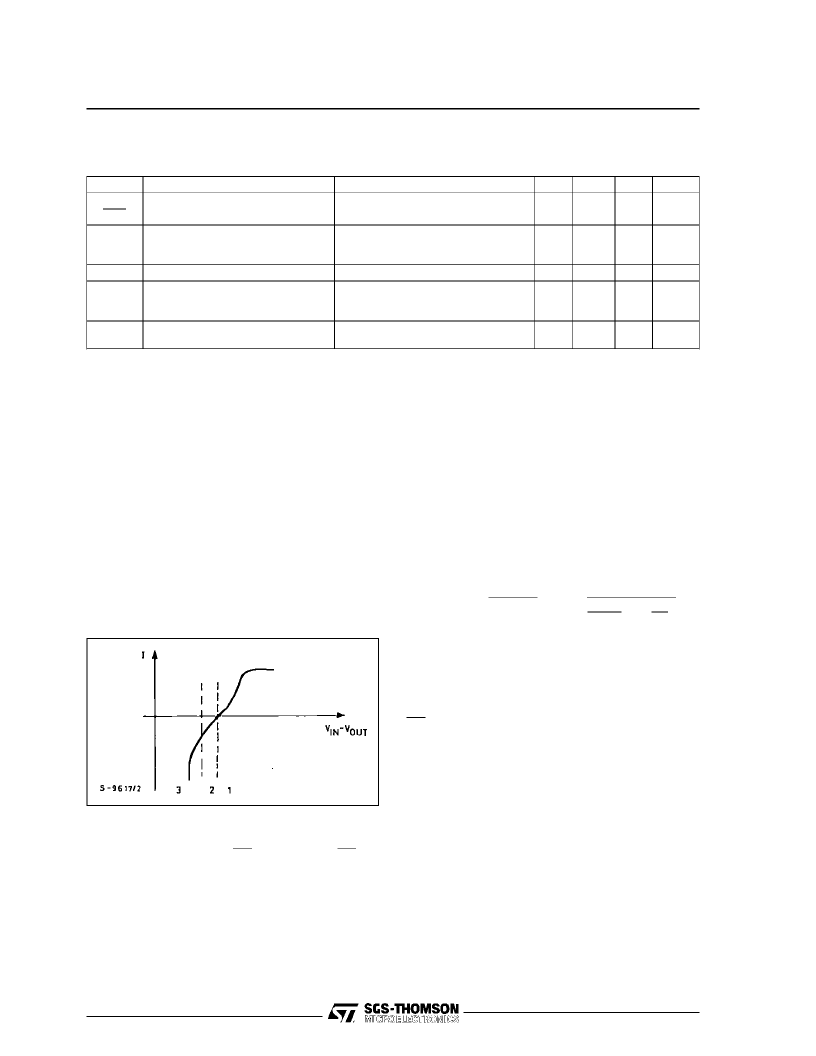
In this conditionthe device works in the range (1)
of the characteristic of the non linear drop control
unit (see Figure 1).
Figure 1 :
Nonliner Transfer Characteristic of
the Drop ControlUnit
The output voltageis fixed to itsnominal value :
V
OUT
NOM
=
V
REF
The ripple rejection is quite high (70dB) and inde-
pendent to C
FT
value.
On the usual voltage regulators, when the input
vol-tage goes belowthe nominalvalue, the regula-
tion transistors (series element) saturate bringing
the system out of regulation and making it very
sensibleto everyvariationof theinput voltage. On
1
+
R1
R2
=
V
CFT
1
+
R1
R2
the contrary,a control loop on theL4915 consents
to avoid the saturation of the series element by
regulating the value of the reference voltage
(pin 2). In fact, whenever the input voltage de-
creasesbelow (V
I MIN
the supervisorloop, utilizing
a non linear OTA, forces the reference voltage at
pin 2 to decrease by discharging C
FT
. So, during
the staticmode,whentheinputvoltagegoesbelow
V
MIN
thedropoutiskept fixedto about1.6 V. Inthis
condition the device works as a low pass filter in
the range (2) of the OTAcharacteristic. The ripple
rejection is externallyadjustableacting on C
FT
as
follows:
SVR
(
j
) =
V
i
(
j
)
V
OUT
(
j
)
=
1
+
10
6
gm
jw C
FT
1
+
R1
R2
Where:
gm =
=
2
10
-5
-1
OTA’S typical transconductancevalue on
linear region
= fixed ratio
R1
R2
C
FT
= value of capacitorin
μ
F
The reactiontime of the supervisorloop isgivenby
the transconductanceoftheOTAandbyC
FT
. When
the value of the ripple voltage is so high and its
negativepeakis fast enoughto determineanistan-
taneousdecrease of the dropouttill 1.2V,the OTA
works in a higher transconductance condition
[range (3) of the characteristic] anddischargesthe
capacitorrapidously.
If theripple frequencyis high enoughthecapacitor
won’tcharge itself completely, andthe outputvolt-
age reaches a smallvalue allowing a betterripple
rejection; thedevice’sagainworking asafilter (fast
transientrange).
With C
FT
=10
μ
F; f = 100Hz; V
o
= 8.5Va SVRof 35
is obtained.
L4915
3/7
相關(guān)PDF資料 |
PDF描述 |
|---|---|
| L4916 | VOLTAGE REGULATOR PLUS FILTER |
| L4918 | VOLTAGE REGULATORS PLUS FILTER |
| L4920 | Very Lowdrop Adjustable Regulators(低壓差輸出可調(diào)穩(wěn)壓器) |
| L4921 | Very Lowdrop Adjustable Regulators(低壓差輸出可調(diào)穩(wěn)壓器) |
| L4922 | Very Lowdrop Adjustable Regulators(帶復(fù)位的低壓差穩(wěn)壓器) |
相關(guān)代理商/技術(shù)參數(shù) |
參數(shù)描述 |
|---|---|
| L4915B | 制造商:RICHARDSON ELECTRONICS 功能描述:HYDROGEN THYRATRON |
| L4916 | 功能描述:線性穩(wěn)壓器 - 標(biāo)準(zhǔn) 8.5V 0.25A w/Filter RoHS:否 制造商:STMicroelectronics 輸出類型: 極性: 輸出電壓:1.8 V 輸出電流:150 mA 負(fù)載調(diào)節(jié): 最大輸入電壓:5.5 V 線路調(diào)整率: 最大工作溫度:+ 125 C 安裝風(fēng)格:SMD/SMT 封裝 / 箱體:SOT-323-5L |
| L4918 | 功能描述:線性穩(wěn)壓器 - 標(biāo)準(zhǔn) 8.5V 0.25A w/Filter RoHS:否 制造商:STMicroelectronics 輸出類型: 極性: 輸出電壓:1.8 V 輸出電流:150 mA 負(fù)載調(diào)節(jié): 最大輸入電壓:5.5 V 線路調(diào)整率: 最大工作溫度:+ 125 C 安裝風(fēng)格:SMD/SMT 封裝 / 箱體:SOT-323-5L |
| L492 | 制造商:未知廠家 制造商全稱:未知廠家 功能描述:THYRISTOR MODULE|SCR|DUAL|INDEPENDENT|240V V(RRM)|22A I(T) |
| L4920 | 制造商:SGS Thomson 功能描述:LDO Regulator Pos 1.25V to 20V 0.8A 5-Pin(5+Tab) PENTAWATT |
發(fā)布緊急采購(gòu),3分鐘左右您將得到回復(fù)。