- 您現(xiàn)在的位置:買(mǎi)賣(mài)IC網(wǎng) > PDF目錄224105 > L415-044.736M (CONNOR WINFIELD CORP) CRYSTAL OSCILLATOR, CLOCK, 44.736 MHz, LVDS OUTPUT PDF資料下載
參數(shù)資料
| 型號(hào): | L415-044.736M |
| 廠商: | CONNOR WINFIELD CORP |
| 元件分類: | XO, clock |
| 英文描述: | CRYSTAL OSCILLATOR, CLOCK, 44.736 MHz, LVDS OUTPUT |
| 封裝: | ROHS COMPLIANT, HERMETIC SEALED, CERAMIC PACKAGE-6 |
| 文件頁(yè)數(shù): | 2/2頁(yè) |
| 文件大小: | 171K |
| 代理商: | L415-044.736M |
Specifications subject to change without notice. All dimensions in inches. Copyright 2009 The Connor-Winfield Corporation
2111 Comprehensive Drive
Aurora, Illinois 60505
Phone: 630- 851- 4722
Fax: 630- 851- 5040
www.conwin.com
Bulletin
Ds021
Page
2 of 2
Revision
08
Date
02 Dec 2009
Dimensional Tolerance: ±.02” (.508mm)
±.005” (.127mm)
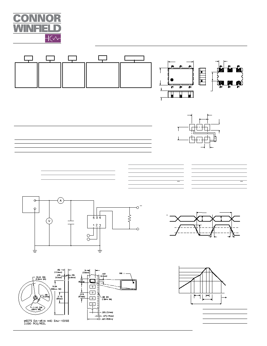
Suggested Pad Layout
Output Waveform
Tape and Reel Dimensions
Environmental Characteristics
Vibration:
Vibration per Mil Std 883E Method 2007.3 Test Condition A.
Shock:
Mechanical Shock per Mil Std 883E Method 2002.4 Test Condition B.
Soldering Process; RoHS compliant lead free. See soldering profile on page 2.
Solderability;
Solderability per Mil Std 883E Method 2003.
Models: Lxx4, Lxx5
1:
N/C
2
Enable / Disable
3:
Ground
4:
Output Q
5:
Complementary Output Q
6:
Supply Voltage (Vcc)
Pad Connections
Function:
Output
Low:
Disabled (High Impedance)
High or Open: Enabled
Solder Profile
120°C
150°C
180°C
260°C
0
220°C
360 Sec. Max.
120 S
Max.
10 S
60 S
Max.
Time
Temperature
260°C
Enable / Disable Function
0.200
(5.08mm)
0.100
(2.54mm)
0.079
(2.0mm)
0.165
(4.2mm)
0.070
(1.78mm)
Bypass
Capacitor
0.01uF
Ground
Top
View
4
5
6
3
2
1
Vod
Duty Cycle
Vod
0V
80%
20%
Vopp
t r
t f
Q
Differential
Output
Waveform
peak-to-peak
CW 0946
L143
155.52M
.059
(1.50mm)
0.275
(7.0mm)
0.197
(5.0mm)
0.102
(2.6mm)
0.055
(1.4mm)
Dimensional Tolerance
+/-0.008 (+/-0.2mm)
Vcc
Power
Supply
Ground
Enable /
Disable
or N/C
0.01 uF
100
Ohm
Q
Package Characteristics
Package
Hermetically sealed ceramic package and metal cover
Type
LVDS
Clock Series
5x7mm
Temperature
Range
1 = 0 to 70°C
2 = -40 to 85°C
3 = 0 to 85°C
4 = -20 to 70°C
Frequency
Stability
4 = ±20 ppm
1 = ±25 ppm
2 = ±50 ppm
3 = ±100 ppm
Output Frequency
Frequency Format
-xxx.xM Min
-xxx.xxxxxxM Max
*Amount of numbers
after the decimal
point. M = MHz
L
1
4
- 155.52M
Supply Voltage
2 = 2.5 Vdc, E/D Pad 1
3 = 3.3 Vdc, E/D Pad 1
4 = 2.5 Vdc, E/D Pad 2
5 = 3.3 Vdc, E/D Pad 2
3
Ordering Information
Package Outline
Example: Part Number
L143-155.52M = LVDS Output,
0 to 70, +/-20ppm, 3.3Vdc, E/D Pad 1, Output Frequency 155.52MHz
To order an L143 with an output frequency of:
25 MHz = L143-025.0M
44.736 MHz = L143-044.736M
155.52 MHz = L143-155.52M
Test Circuit
Models: Lxx2, Lxx3
1:
Enable / Disable
2
N/C
3:
Ground
4:
Output Q
5:
Complementary Output Q
6:
Supply Voltage (Vcc)
相關(guān)PDF資料 |
PDF描述 |
|---|---|
| L1384AD/SRD | SINGLE COLOR LED, SUPER BRIGHT RED, 3.4 mm |
| L145-260.0M | CRYSTAL OSCILLATOR, CLOCK, 260 MHz, LVDS OUTPUT |
| L315-260.0M | CRYSTAL OSCILLATOR, CLOCK, 260 MHz, LVDS OUTPUT |
| L335-260.0M | CRYSTAL OSCILLATOR, CLOCK, 260 MHz, LVDS OUTPUT |
| L423-260.0M | CRYSTAL OSCILLATOR, CLOCK, 260 MHz, LVDS OUTPUT |
相關(guān)代理商/技術(shù)參數(shù) |
參數(shù)描述 |
|---|---|
| L415-155.52 | 制造商:CONNOR-WINFIELD 制造商全稱:Connor-Winfield Corporation 功能描述:5.0x7.0mm Surface Mount LVDS Clock Oscillator Series |
| L416 | 制造商:未知廠家 制造商全稱:未知廠家 功能描述:L-series platinum temperature sensors are characterized by long-term stability |
| L416000XFCB20BX | 制造商:Precision Devices Inc 功能描述: |
| L416000XFCD20BB | 制造商:PRECISION 功能描述: |
| L416000XFCD20BX | 制造商:Precision Devices Inc 功能描述:16.000Mhz Crystal |
發(fā)布緊急采購(gòu),3分鐘左右您將得到回復(fù)。