- 您現(xiàn)在的位置:買(mǎi)賣(mài)IC網(wǎng) > PDF目錄373127 > KFH2G16U2M-DID6 (SAMSUNG SEMICONDUCTOR CO. LTD.) FLASH MEMORY(54MHz) PDF資料下載
參數(shù)資料
| 型號(hào): | KFH2G16U2M-DID6 |
| 廠(chǎng)商: | SAMSUNG SEMICONDUCTOR CO. LTD. |
| 英文描述: | FLASH MEMORY(54MHz) |
| 中文描述: | 閃存(54MHz之間) |
| 文件頁(yè)數(shù): | 77/125頁(yè) |
| 文件大?。?/td> | 1657K |
| 代理商: | KFH2G16U2M-DID6 |
第1頁(yè)第2頁(yè)第3頁(yè)第4頁(yè)第5頁(yè)第6頁(yè)第7頁(yè)第8頁(yè)第9頁(yè)第10頁(yè)第11頁(yè)第12頁(yè)第13頁(yè)第14頁(yè)第15頁(yè)第16頁(yè)第17頁(yè)第18頁(yè)第19頁(yè)第20頁(yè)第21頁(yè)第22頁(yè)第23頁(yè)第24頁(yè)第25頁(yè)第26頁(yè)第27頁(yè)第28頁(yè)第29頁(yè)第30頁(yè)第31頁(yè)第32頁(yè)第33頁(yè)第34頁(yè)第35頁(yè)第36頁(yè)第37頁(yè)第38頁(yè)第39頁(yè)第40頁(yè)第41頁(yè)第42頁(yè)第43頁(yè)第44頁(yè)第45頁(yè)第46頁(yè)第47頁(yè)第48頁(yè)第49頁(yè)第50頁(yè)第51頁(yè)第52頁(yè)第53頁(yè)第54頁(yè)第55頁(yè)第56頁(yè)第57頁(yè)第58頁(yè)第59頁(yè)第60頁(yè)第61頁(yè)第62頁(yè)第63頁(yè)第64頁(yè)第65頁(yè)第66頁(yè)第67頁(yè)第68頁(yè)第69頁(yè)第70頁(yè)第71頁(yè)第72頁(yè)第73頁(yè)第74頁(yè)第75頁(yè)第76頁(yè)當(dāng)前第77頁(yè)第78頁(yè)第79頁(yè)第80頁(yè)第81頁(yè)第82頁(yè)第83頁(yè)第84頁(yè)第85頁(yè)第86頁(yè)第87頁(yè)第88頁(yè)第89頁(yè)第90頁(yè)第91頁(yè)第92頁(yè)第93頁(yè)第94頁(yè)第95頁(yè)第96頁(yè)第97頁(yè)第98頁(yè)第99頁(yè)第100頁(yè)第101頁(yè)第102頁(yè)第103頁(yè)第104頁(yè)第105頁(yè)第106頁(yè)第107頁(yè)第108頁(yè)第109頁(yè)第110頁(yè)第111頁(yè)第112頁(yè)第113頁(yè)第114頁(yè)第115頁(yè)第116頁(yè)第117頁(yè)第118頁(yè)第119頁(yè)第120頁(yè)第121頁(yè)第122頁(yè)第123頁(yè)第124頁(yè)第125頁(yè)
OneNAND1G(KFG1G16Q2M-DEB5)
FLASH MEMORY
77
OneNAND2G(KFH2G16Q2M-DEB5)
OneNAND4G(KFW4G16Q2M-DEB5)
When the CE or OE input is at V
IH
, output from the device is disabled.
The outputs are placed in the high impedance state.
The Program operation is used to program data from the on-chip BufferRAMs into the NAND FLASH memory array.
The device has two 2KB data buffers, each 1 Page (2KB + 64B) in size. Each page has 4 sectors of 512B each main area and 16B
spare area. The device can be programmed in units of 1~4 sectors.
The architecture of the DataRAMs permits a simultaneous data-write operation from the Host to one of data buffers and a program
operation from the other data buffer to the NAND Flash Array memory. Refer to Section 3.12.2, "Write While Program Operation", for
more information.
3.8 Program Operation
See Timing Diagram 6.9
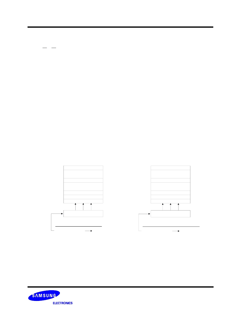
Within a block, the pages must be programmed consecutively from the LSB (least significant bit) page of the block to MSB (most sig-
nificant bit) pages of the block. Random page address programming is prohibited.
From the LSB page to MSB page
DATA IN: Data (1)
Data (64)
(1)
(2)
(3)
(32)
(64)
Data register
Page 0
Page 1
Page 2
Page 31
Page 63
Ex.) Random page program (Prohibition)
DATA IN: Data (1)
Data (64)
(2)
(32)
(3)
(1)
(64)
Data register
Page 0
Page 1
Page 2
Page 31
Page 63
Addressing for program operation
:
:
:
:
3.7.4 Output Disable Mode Operation
相關(guān)PDF資料 |
PDF描述 |
|---|---|
| KFH4G1612M-DEB5 | FLASH MEMORY(54MHz) |
| KFH4G1612M-DED5 | FLASH MEMORY(54MHz) |
| KFH4G16D2M-DEB5 | FLASH MEMORY(54MHz) |
| KFH4G16D2M-DEB6 | FLASH MEMORY(54MHz) |
| KFH4G16D2M-DED5 | FLASH MEMORY(54MHz) |
相關(guān)代理商/技術(shù)參數(shù) |
參數(shù)描述 |
|---|---|
| KFH-440-10 | 制造商:PennEngineering (PEM) 功能描述: |
| KFH-440-12ET | 制造商:PennEngineering (PEM) 功能描述: |
| KFH4405 | 制造商:n/a 功能描述:Ships in 2 days |
| KFH-440-5ET | 制造商:PennEngineering (PEM) 功能描述: |
| KFH4406 | 制造商:n/a 功能描述:Ships in 2 days |
發(fā)布緊急采購(gòu),3分鐘左右您將得到回復(fù)。