- 您現(xiàn)在的位置:買賣IC網(wǎng) > PDF目錄374296 > K9F2808U0B-D (SAMSUNG SEMICONDUCTOR CO. LTD.) 16M x 8 Bit NAND Flash Memory PDF資料下載
參數(shù)資料
| 型號(hào): | K9F2808U0B-D |
| 廠商: | SAMSUNG SEMICONDUCTOR CO. LTD. |
| 英文描述: | 16M x 8 Bit NAND Flash Memory |
| 中文描述: | 1,600 × 8位NAND閃存 |
| 文件頁(yè)數(shù): | 9/29頁(yè) |
| 文件大?。?/td> | 304K |
| 代理商: | K9F2808U0B-D |
第1頁(yè)第2頁(yè)第3頁(yè)第4頁(yè)第5頁(yè)第6頁(yè)第7頁(yè)第8頁(yè)當(dāng)前第9頁(yè)第10頁(yè)第11頁(yè)第12頁(yè)第13頁(yè)第14頁(yè)第15頁(yè)第16頁(yè)第17頁(yè)第18頁(yè)第19頁(yè)第20頁(yè)第21頁(yè)第22頁(yè)第23頁(yè)第24頁(yè)第25頁(yè)第26頁(yè)第27頁(yè)第28頁(yè)第29頁(yè)
FLASH MEMORY
9
K9F2808U0B-YCB0,YIB0
K9F2808U0B-DCB0,DIB0
K9F2808Q0B-DCB0,DIB0
K9F2808U0B-VCB0,VIB0
PRODUCT INTRODUCTION
The K9F2808X0B is a 132Mbit(138,412,032 bit) memory organized as 32,768 rows(pages) by 528 columns. Spare 16 columns are
located in 512 to 527 column address. A 528-byte data register is connected to memory cell arrays accommodating data transfer
between the I/O buffers and memory during page read and page program operations. The memory array is made up of 16 cells that
are serially connected like NAND structure. Each of the 16 cells resides in a different page. A block consists of the 32 pages formed
by one NAND structures, totaling 8448 NAND structures of 16 cells. The array organization is shown in Figure 2. Program and read
operations are executed on a page basis, while erase operation is executed on a block basis. The memory array consists of 1024
blocks, and a block is separately erasable by 16K-byte unit. It indicates that the bit by bit erase operation is prohibited on the
K9F2808X0B.
The K9F2808X0B has addresses multiplexed with 8 I/O
′
s. This scheme dramatically reduces pin counts and allows systems
upgrades to future densities by maintaining consistency in system board design. Command, address and data are all written through
I/O
′
s by bringing WE to low while CE is low. Data is latched on the rising edge of WE. Command Latch Enable(CLE) and Address
Latch Enable(ALE) are used to multiplex command and address respectively, via the I/O pins. All commands require one bus cycle
except Page Program command and Block Erase command which require two cycles: one cycle for setup and another for execution.
The 16M byte physical space requires 24 addresses, thereby requiring three cycles for byte-level addressing: column address, low
row address and high row address, in that order. Page Read and Page Program need the same three address cycles following
required command input. In Block Erase operation, however, only two row address cycles are used. Device operations are selected
by writing specific commands into command register. Table 1 defines the specific commands of the K9F2808X0B.
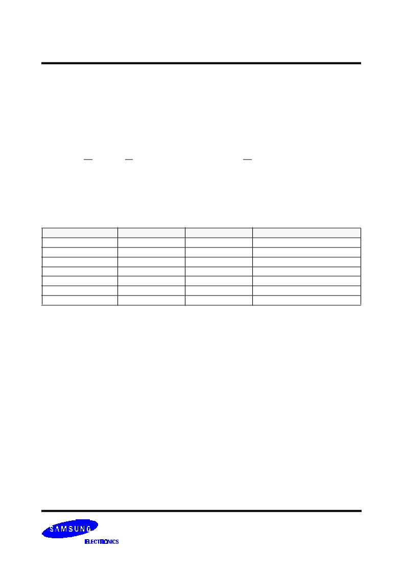
Table 1. COMMAND SETS
NOTE
: 1. The 00h command defines starting address of the 1st half of registers.
The 01h command defines starting address of the 2nd half of registers.
After data access on 2nd half of register by the 01h command, start pointer is automatically moved to
1st half register(00h) on the next cycle.
Caution
: Any undefined command inputs are prohibited except for above command set of Table 1.
Function
1st. Cycle
2nd. Cycle
Acceptable Command during Busy
Read 1
00h/01h
(1)
-
Read 2
50h
-
Read ID
90h
-
Reset
FFh
-
O
Page Program
80h
10h
Block Erase
60h
D0h
Read Status
70h
-
O
相關(guān)PDF資料 |
PDF描述 |
|---|---|
| K9F2808U0B-V | 16M x 8 Bit NAND Flash Memory |
| K9F2808U0B-VCB0 | 16M x 8 Bit NAND Flash Memory |
| K9F2808U0B-Y | 16M x 8 Bit NAND Flash Memory |
| K9F2808U0C-VCB0 | 16M x 8 Bit , 8M x 16 Bit NAND Flash Memory |
| K9F2808U0C-DCB0 | 16M x 8 Bit , 8M x 16 Bit NAND Flash Memory |
相關(guān)代理商/技術(shù)參數(shù) |
參數(shù)描述 |
|---|---|
| K9F2808U0B-DCB0 | 制造商:SAMSUNG 制造商全稱:Samsung semiconductor 功能描述:16M x 8 Bit NAND Flash Memory |
| K9F2808U0B-DIB0 | 制造商:SAMSUNG 制造商全稱:Samsung semiconductor 功能描述:16M x 8 Bit NAND Flash Memory |
| K9F2808U0B-V | 制造商:SAMSUNG 制造商全稱:Samsung semiconductor 功能描述:16M x 8 Bit NAND Flash Memory |
| K9F2808U0B-VCB0 | 制造商:SAMSUNG 制造商全稱:Samsung semiconductor 功能描述:16M x 8 Bit NAND Flash Memory |
| K9F2808U0B-VIB0 | 制造商:SAMSUNG 制造商全稱:Samsung semiconductor 功能描述:16M x 8 Bit NAND Flash Memory |
發(fā)布緊急采購(gòu),3分鐘左右您將得到回復(fù)。