- 您現(xiàn)在的位置:買賣IC網 > PDF目錄374296 > K9F1608W0A- (SAMSUNG SEMICONDUCTOR CO. LTD.) 2M x 8 Bit NAND Flash Memory PDF資料下載
參數資料
| 型號: | K9F1608W0A- |
| 廠商: | SAMSUNG SEMICONDUCTOR CO. LTD. |
| 英文描述: | 2M x 8 Bit NAND Flash Memory |
| 中文描述: | 200萬× 8位NAND閃存 |
| 文件頁數: | 9/25頁 |
| 文件大小: | 443K |
| 代理商: | K9F1608W0A- |
K9F1608W0A-TCB0, K9F1608W0A-TIB0
FLASH MEMORY
9
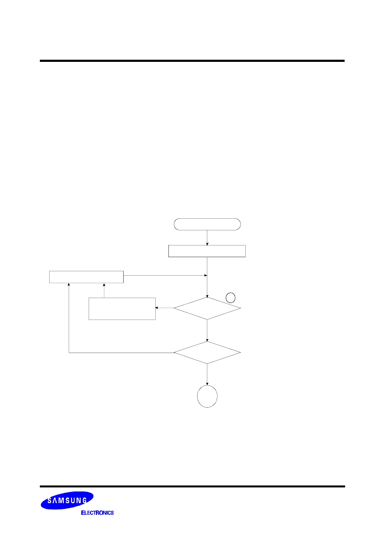
Identifying Invalid Block(s)
All device locations are erased(FFh) except locations where the invalid block information is written prior to shipping.
Since the
invalid block information is also erasable in most cases, it is impossible to recover the information once it has been
erased. Therefore, the system must be able to recognize the invalid block(s) based on the original invalid block
information and create the invalid block table via the following suggested flow chart(Figure 1). Any intentional era-
sure of the original invalid block information is prohibited.
Invalid Block(s)
Invalid blocks are defined as blocks that contain one or more invalid bits whose reliability is not guaranteed by Samsung. Typically,
an invalid block will contain a single bad bit. The information regarding the invalid block(s) is called as the invalid block information.
The invalid block information is written to the 1st or the 2nd page of the invalid block(s) with 00h data.
Devices with invalid block(s)
have the same quality level or as devices with all valid blocks and have the same AC and DC characteristics. An invalid block(s)
does not affect the performance of valid block(s) because it is isolated from the bit line and the common source line by a select tran-
sistor. The system design must be able to mask out the invalid block(s) via address mapping. The 1st block of the NAND Flash, how-
ever, is fully guaranteed to be a valid block.
NAND Flash Technical Notes
*
Check "FFH" on the 1st and 2nd page
Figure 1. Flow chart to create invalid block table.
Start
Set Block Address = 0
Check "FFH"
Increment Block Address
Last Block
End
No
Yes
Yes
Create (or update)
Invalid Block(s) Table
No
相關PDF資料 |
PDF描述 |
|---|---|
| K9F1608W0A-TCB0 | TV 128C 128#22D SKT RECP |
| K9F1608W0A-TIB0 | TV 37C 37#16 PIN RECP |
| K9F1G08Q0A | FLASH MEMORY |
| K9F1G08U0A | FLASH MEMORY |
| K9F1G08Q0M-YIB0 | 1Gb Gb 1.8V NAND Flash Errata |
相關代理商/技術參數 |
參數描述 |
|---|---|
| K9F1608W0A-TCB0 | 制造商:SAMSG 功能描述: |
| K9F1608W0A-TIB0 | 制造商:SAMSUNG 制造商全稱:Samsung semiconductor 功能描述:2M x 8 Bit NAND Flash Memory |
| K9F1G08B0C-PCB0T00 | 制造商:Samsung Semiconductor 功能描述:1GB SLC NORMAL X8 FBGA - Trays |
| K9F1G08D0M | 制造商:SAMSUNG 制造商全稱:Samsung semiconductor 功能描述:128M x 8 Bit / 64M x 16 Bit NAND Flash Memory |
| K9F1G08Q0A | 制造商:SAMSUNG 制造商全稱:Samsung semiconductor 功能描述:FLASH MEMORY |
發(fā)布緊急采購,3分鐘左右您將得到回復。