- 您現(xiàn)在的位置:買賣IC網(wǎng) > PDF目錄374277 > K4R881869M (SAMSUNG SEMICONDUCTOR CO. LTD.) 288Mbit RDRAM 512K x 18 bit x 2*16 Dependent Banks Direct RDRAMTM PDF資料下載
參數(shù)資料
| 型號(hào): | K4R881869M |
| 廠商: | SAMSUNG SEMICONDUCTOR CO. LTD. |
| 英文描述: | 288Mbit RDRAM 512K x 18 bit x 2*16 Dependent Banks Direct RDRAMTM |
| 中文描述: | 288Mbit RDRAM的為512k × 18位× 2 * 16屬銀行直接RDRAMTM |
| 文件頁(yè)數(shù): | 42/64頁(yè) |
| 文件大小: | 4084K |
| 代理商: | K4R881869M |
第1頁(yè)第2頁(yè)第3頁(yè)第4頁(yè)第5頁(yè)第6頁(yè)第7頁(yè)第8頁(yè)第9頁(yè)第10頁(yè)第11頁(yè)第12頁(yè)第13頁(yè)第14頁(yè)第15頁(yè)第16頁(yè)第17頁(yè)第18頁(yè)第19頁(yè)第20頁(yè)第21頁(yè)第22頁(yè)第23頁(yè)第24頁(yè)第25頁(yè)第26頁(yè)第27頁(yè)第28頁(yè)第29頁(yè)第30頁(yè)第31頁(yè)第32頁(yè)第33頁(yè)第34頁(yè)第35頁(yè)第36頁(yè)第37頁(yè)第38頁(yè)第39頁(yè)第40頁(yè)第41頁(yè)當(dāng)前第42頁(yè)第43頁(yè)第44頁(yè)第45頁(yè)第46頁(yè)第47頁(yè)第48頁(yè)第49頁(yè)第50頁(yè)第51頁(yè)第52頁(yè)第53頁(yè)第54頁(yè)第55頁(yè)第56頁(yè)第57頁(yè)第58頁(yè)第59頁(yè)第60頁(yè)第61頁(yè)第62頁(yè)第63頁(yè)第64頁(yè)
Page 40
Direct RDRAM
K4R881869M
Rev. 0.9 Jan. 2000
Preliminary
PDEV5..0 address packet and exits NAP or PDN when the
wake-up sequence is presented on the CMD wire. The ROW
and COL pins must be quiet at a time t
S4
/t
H4
around the indi-
cated falling SCK edge (timed with the PDNX or NAPX
register fields). After that, ROW and COL packets may be
directed to the RDRAM which is now in ATTN or STBY
state.
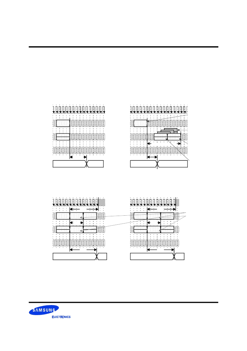
Figure 49 shows the constraints for entering and exiting
NAP and PDN states. On the left side, an RDRAM exits
NAP state at the end of cycle T
3
. This RDRAM may not re-
enter NAP or PDN state for an interval of t
NU0
. The
RDRAM enters NAP state at the end of cycle T
13
. This
RDRAM may not re-exit NAP state for an interval of t
NU1
.
The equations for these two parameters depend upon a
number of factors, and are shown at the bottom of the figure.
NAPX is the value in the NAPX field in the NAPX register.
On the right side of Figure 48, an RDRAM exits PDN state
at the end of cycle T
3
. This RDRAM may not re-enter PDN
or NAP state for an interval of t
PU0
. The RDRAM enters
PDN state at the end of cycle T
13
. This RDRAM may not re-
exit PDN state for an interval of t
PU1
. The equations for
these two parameters depend upon a number of factors, and
are shown at the bottom of the figure. PDNX is the value in
the PDNX field in the PDNX register.
Figure 46: STBY Entry (left) and STBY Exit (right)
STBY
ATTN
CTM/CFM
DQA8..0
DQB8..0
COL4
..COL0
ROW2
..ROW0
T
0
T
4
T
8
T
12
T
1
T
5
T
9
T
13
T
2
T
6
T
10
T
14
T
3
T
7
T
11
T
15
T
16
T
20
T
17
T
21
T
18
T
22
T
19
23
T
0
CTM/CFM
DQA8..0
DQB8..0
COL4
..COL0
ROW2
..ROW0
T
4
T
8
T
12
T
1
T
5
T
9
T
13
T
2
T
6
T
10
T
14
T
3
T
7
T
11
T
15
T
16
T
20
T
17
T
21
T
18
T
22
T
19
T
23
t
AS
RLXR
Power
State
ATTN
Power
State
STBY
t
SA
ROP a0
RLXC
RLXX
TFRMt
CYCLE
ROP = non-broadcast ROWA
or ROWR/ATTN
a0 = {d0,b0,r0}
a1 = {d1,b1,c1}
No COL packets may be
placed in the three
indicated positions; i.e. at
(TFRM - {1,2,3})t
CYCLE
.
A COL packet to device d0
(or any other device) is okay
at
(TFRM)t
CYCLE
or later.
A COL packet to another
device (d1!= d0) is okay at
(TFRM - 4)t
CYCLE
or earlier.
XXXXXOP a0
CCCCOP a1
Figure 47: NAP Entry (left) and PDN Entry (right)
CTM/CFM
DQA8..0
DQB8..0
COL4
..COL0
ROW2
..ROW0
T
0
T
4
T
8
T
12
T
1
T
5
T
9
T
13
T
2
T
6
T
10
T
14
T
3
T
7
T
11
T
15
T
16
T
20
T
17
T
21
T
18
T
22
T
19
23
T
0
CTM/CFM
DQA8..0
DQB8..0
COL4
..COL0
ROW2
..ROW0
T
4
T
8
T
12
T
1
T
5
T
9
T
13
T
2
T
6
T
10
T
14
T
3
T
7
T
11
T
15
T
16
T
20
T
17
T
21
T
18
T
22
T
19
T
23
ROP a0
(NAPR)
Power
State
Power
State
a
The (eventual) NAP/PDN exit will be to the same ATTN/STBY state the RDRAM was in prior to NAP/PDN entry
t
CD
ROP a1
COP a0
XOP a0
COP a1
XOP a1
t
ASN
ATTN/STBY
a
NAP
ROP a0
(PDNR)
ROP a1
COP a0
XOP a0
COP a1
XOP a1
t
ASP
ATTN/STBY
a
PDN
t
CD
t
NPQ
restricted
t
NPQ
restricted
restricted
restricted
a0 = {d0,b0,r0,c0}
a1 = {d1,b1,r1,c1}
No ROW or COL packets
directed to device d0 may
overlap the restricted
interval. No broadcast ROW
packets may overlap the quiet
interval.
ROW or COL packets to a
device other than d0 may
overlap the restricted
interval.
ROW or COL packets
directed to device d0 after the
restricted interval will be
ignored.
相關(guān)PDF資料 |
PDF描述 |
|---|---|
| K4R881869M-NbCcG6 | 288Mbit RDRAM 512K x 18 bit x 2*16 Dependent Banks Direct RDRAMTM |
| K4R881869M-NCK7 | 288Mbit RDRAM 512K x 18 bit x 2*16 Dependent Banks Direct RDRAMTM |
| K4R881869M-NCK8 | 288Mbit RDRAM 512K x 18 bit x 2*16 Dependent Banks Direct RDRAMTM |
| K4S280432A | 128Mbit SDRAM 8M x 4Bit x 4 Banks Synchronous DRAM LVTTL |
| K4S280432C | 128Mbit SDRAM 8M x 4Bit x 4 Banks Synchronous DRAM LVTTL |
相關(guān)代理商/技術(shù)參數(shù) |
參數(shù)描述 |
|---|---|
| K4R881869M-NBCCG6 | 制造商:SAMSUNG 制造商全稱:Samsung semiconductor 功能描述:288Mbit RDRAM 512K x 18 bit x 2*16 Dependent Banks Direct RDRAMTM |
| K4R881869M-NCK7 | 制造商:SAMSUNG 制造商全稱:Samsung semiconductor 功能描述:288Mbit RDRAM 512K x 18 bit x 2*16 Dependent Banks Direct RDRAMTM |
| K4R881869M-NCK8 | 制造商:SAMSUNG 制造商全稱:Samsung semiconductor 功能描述:288Mbit RDRAM 512K x 18 bit x 2*16 Dependent Banks Direct RDRAMTM |
| K4R881869M-NCK8000 | 制造商:Samsung SDI 功能描述: |
| K4S160822D | 制造商:SAMSUNG 制造商全稱:Samsung semiconductor 功能描述:2Mx8 SDRAM 1M x 8bit x 2 Banks Synchronous DRAM LVTTL |
發(fā)布緊急采購(gòu),3分鐘左右您將得到回復(fù)。