- 您現在的位置:買賣IC網 > PDF目錄373065 > K4N56163QF-GC25 (SAMSUNG SEMICONDUCTOR CO. LTD.) 256Mbit gDDR2 SDRAM PDF資料下載
參數資料
| 型號: | K4N56163QF-GC25 |
| 廠商: | SAMSUNG SEMICONDUCTOR CO. LTD. |
| 英文描述: | 256Mbit gDDR2 SDRAM |
| 中文描述: | 片256Mbit GDDR2 SDRAM的 |
| 文件頁數: | 37/73頁 |
| 文件大?。?/td> | 1262K |
| 代理商: | K4N56163QF-GC25 |
第1頁第2頁第3頁第4頁第5頁第6頁第7頁第8頁第9頁第10頁第11頁第12頁第13頁第14頁第15頁第16頁第17頁第18頁第19頁第20頁第21頁第22頁第23頁第24頁第25頁第26頁第27頁第28頁第29頁第30頁第31頁第32頁第33頁第34頁第35頁第36頁當前第37頁第38頁第39頁第40頁第41頁第42頁第43頁第44頁第45頁第46頁第47頁第48頁第49頁第50頁第51頁第52頁第53頁第54頁第55頁第56頁第57頁第58頁第59頁第60頁第61頁第62頁第63頁第64頁第65頁第66頁第67頁第68頁第69頁第70頁第71頁第72頁第73頁
- 37 -
Rev 1.6 (Apr. 2005)
256M gDDR2 SDRAM
K4N56163QF-GC
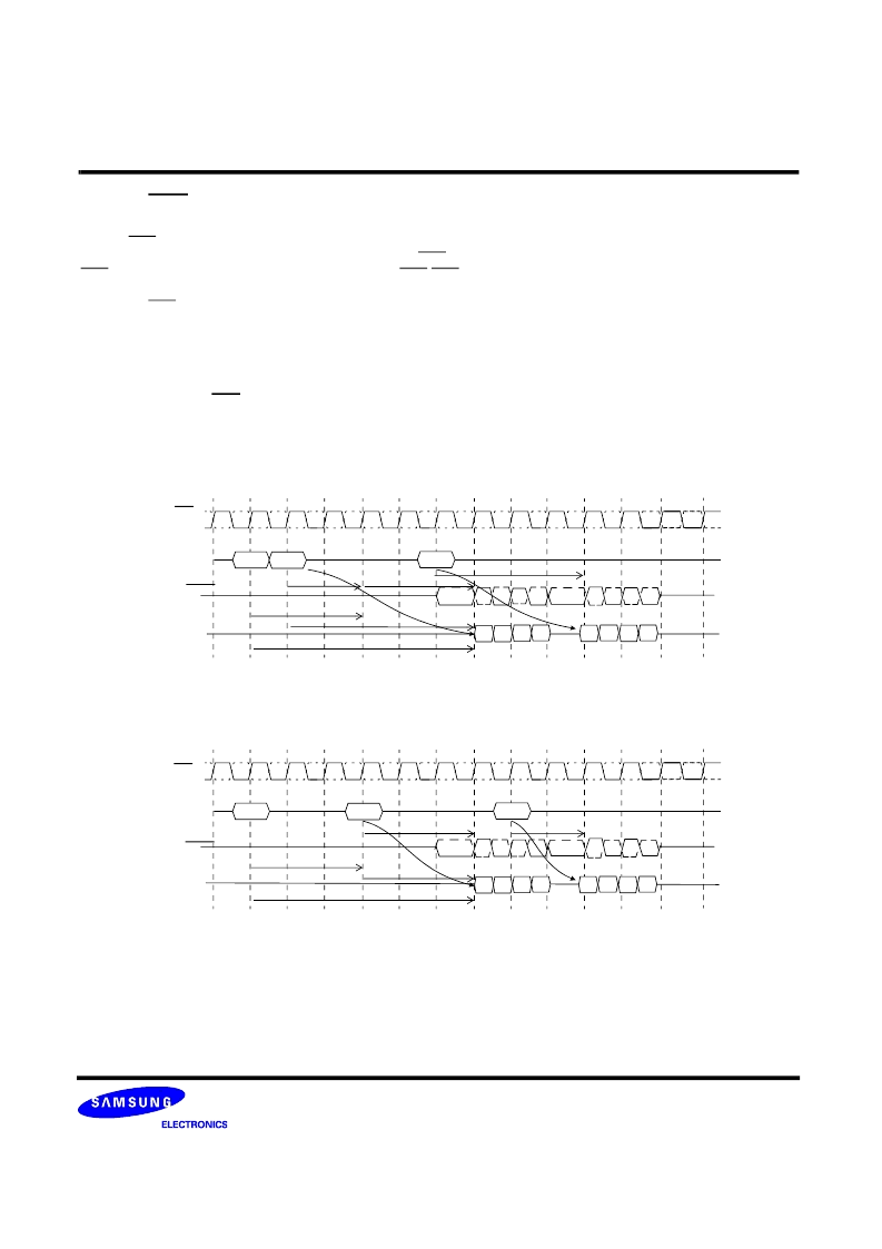
Posted CAS
Posted CAS operation is supported to make command and data bus efficient for sustainable bandwidths in gDDR2
SDRAM. In this operation, the gDDR2 SDRAM allows a CAS read or write command to be issued immediately after the
RAS bank activate command (or any time during the RAS-CAS-delay time, tRCD, period). The command is held for the
time of the Additive Latency (AL) before it is issued inside the device. The Read Latency (RL) is controlled by the sum of
AL and the CAS latency (CL). Therefore if a user chooses to issue a R/W command before the tRCDmin, then AL (greater
than 0) must be written into the EMR(1). The Write Latency (WL) is always defined as RL - 1 (read latency -1) where read
latency is defined as the sum of additive latency plus CAS latency (RL=AL+CL). Read or Write operations using AL allow
seamless bursts (refer to seamless operation timing diagram examples in Read burst and Write burst section)
Examples of posted CAS operation
Example 1 Read followed by a write to the same bank
[AL = 2 and CL = 3, RL = (AL + CL) = 5, WL = (RL - 1) = 4]
Example 2 Read followed by a write to the same bank
[AL = 0 and CL = 3, RL = (AL + CL) = 3, WL = (RL - 1) = 2]
0
1
2
3
4
5
6
7
8
9
10
11
12
Active
A-Bank
Read
A-Bank
Write
A-Bank
Dout0
Dout1
Dout2
Dout3
Din0
Din1
Din2
Din3
CK/CK
CMD
DQS/DQS
DQ
AL = 2
-1
> = tRCD
CL = 3
> = tRAC
WL = RL -1 = 4
RL = AL + CL = 5
Active
A-Bank
Read
A-Bank
Write
A-Bank
Dout0
Dout1
Dout2
Dout3
Din0
Din1
Din2
Din3
AL = 0
> = tRCD
CL = 3
> = tRAC
WL = RL -1 = 2
RL = AL + CL = 3
0
1
2
3
4
5
6
7
8
9
10
11
12
-1
CK/CK
CMD
DQS/DQS
DQ
相關PDF資料 |
PDF描述 |
|---|---|
| K4N56163QF-GC30 | 256Mbit gDDR2 SDRAM |
| K4N56163QF-GC37 | 256Mbit gDDR2 SDRAM |
| K4PE68A | Transient Voltage Suppressor Diodes |
| K4R271669A | 256K x 16/18 bit x 2*16 Dependent Banks Direct RDRAMTM |
| K4R271669A-N(M)CK7 | 256K x 16/18 bit x 2*16 Dependent Banks Direct RDRAMTM |
相關代理商/技術參數 |
參數描述 |
|---|---|
| K4N56163QF-GC30 | 制造商:SAMSUNG 制造商全稱:Samsung semiconductor 功能描述:256Mbit gDDR2 SDRAM |
| K4N56163QF-GC37 | 制造商:SAMSUNG 制造商全稱:Samsung semiconductor 功能描述:256Mbit gDDR2 SDRAM |
| K4N56163QG-ZC2A | 制造商:Samsung Semiconductor 功能描述: |
| K4P24V3 | 制造商:AROMAT 功能描述:REPLAY 700 OHM |
| K4P-24V-3 | 制造商:AROMAT 功能描述:REPLAY 700 OHM |
發(fā)布緊急采購,3分鐘左右您將得到回復。