- 您現(xiàn)在的位置:買賣IC網(wǎng) > PDF目錄374277 > K4N51163QC-ZC2A (SAMSUNG SEMICONDUCTOR CO. LTD.) 512Mbit gDDR2 SDRAM PDF資料下載
參數(shù)資料
| 型號: | K4N51163QC-ZC2A |
| 廠商: | SAMSUNG SEMICONDUCTOR CO. LTD. |
| 英文描述: | 512Mbit gDDR2 SDRAM |
| 中文描述: | 512MB的GDDR2 SDRAM的 |
| 文件頁數(shù): | 43/64頁 |
| 文件大小: | 1420K |
| 代理商: | K4N51163QC-ZC2A |
第1頁第2頁第3頁第4頁第5頁第6頁第7頁第8頁第9頁第10頁第11頁第12頁第13頁第14頁第15頁第16頁第17頁第18頁第19頁第20頁第21頁第22頁第23頁第24頁第25頁第26頁第27頁第28頁第29頁第30頁第31頁第32頁第33頁第34頁第35頁第36頁第37頁第38頁第39頁第40頁第41頁第42頁當前第43頁第44頁第45頁第46頁第47頁第48頁第49頁第50頁第51頁第52頁第53頁第54頁第55頁第56頁第57頁第58頁第59頁第60頁第61頁第62頁第63頁第64頁
- 43 -
Rev 1.5 Oct. 2005
512M gDDR2 SDRAM
K4N51163QC-ZC
The Precharge Command is used to precharge or close a bank that has been activated. The Precharge Command is triggered when
CS, RAS and WE are low and CAS is high at the rising edge of the clock. The Precharge Command can be used to precharge each
bank independently or all banks simultaneously. Three address bits A10, BA0 and BA1 for 256Mb are used to define which bank to pre-
charge when the command is issued.
Minimum Read to precharge command spacing to the same bank = AL + BL/2 clocks.
For the earliest possible precharge, the precharge command may be issued on the rising edge which is “Additive latency(AL) + BL/2
clocks” after a Read command. A new bank active (command) may be issued to the same bank after the RAS precharge time (t
RP
). A
precharge command cannot be issued until t
RAS
is satisfied.
The minimum Read to Precharge spacing has also to satisfy a minimum analog time from the rising clock edge that initiates the last 4-
bit prefetch of a Read to Precharge command. This time is called tRTP (Read to Precharge). For BL = 4 this is the time from the actual
read (AL after the Read command) to Precharge command. For BL = 8 this is the time from AL + 2 clocks after the Read to the Pre-
charge command.
A10
BA1
BA0
Precharged
Bank(s)
Remarks
LOW
LOW
LOW
Bank 0 only
LOW
LOW
HIGH
Bank 1 only
LOW
HIGH
LOW
Bank 2 only
LOW
HIGH
HIGH
Bank 3 only
HIGH
DON’T CARE
DON’T CARE
All Banks
Bank Selection for Precharge by Address Bits
Burst Read Operation Followed by Precharge
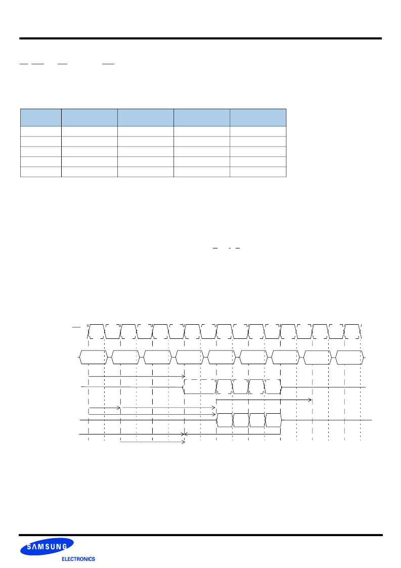
Example 1: Burst Read Operation Followed by Precharge:
RL = 4, AL = 1, CL = 3, BL = 4, t
RTP
<= 2 clocks
CMD
NOP
NOP
Precharge
NOP
DQ’s
NOP
CK/CK
DOUT A
0
DOUT A
1
DOUT A
2
DOUT A
3
READ A
Post CAS
RL =4
DQS
Active
Bank A
> = t
RP
NOP
CL =3
NOP
> = t
RAS
> = t
RTP
T0
T2
T1
T3
T4
T5
T6
T7
T 8
AL + BL/2 clks
AL = 1
CL = 3
Precharge Command
相關PDF資料 |
PDF描述 |
|---|---|
| K4N51163QC-ZC33 | 512Mbit gDDR2 SDRAM |
| K4N51163QC-ZC36 | 512Mbit gDDR2 SDRAM |
| K4R271669B-N(M)CG6 | 256K x 16/18 bit x 32s banks Direct RDRAMTM |
| K4R271669B-N(M)CK7 | 256K x 16/18 bit x 32s banks Direct RDRAMTM |
| K4R271669B-Nb(M)CcK8 | 256K x 16/18 bit x 32s banks Direct RDRAMTM |
相關代理商/技術參數(shù) |
參數(shù)描述 |
|---|---|
| K4N51163QC-ZC33 | 制造商:SAMSUNG 制造商全稱:Samsung semiconductor 功能描述:512Mbit gDDR2 SDRAM |
| K4N51163QC-ZC36 | 制造商:SAMSUNG 制造商全稱:Samsung semiconductor 功能描述:512Mbit gDDR2 SDRAM |
| K4N51163QG | 制造商:SAMSUNG 制造商全稱:Samsung semiconductor 功能描述:Graphic Memory |
| K4N51163QZ | 制造商:SAMSUNG 制造商全稱:Samsung semiconductor 功能描述:Graphic Memory |
| K4N56163QF | 制造商:SAMSUNG 制造商全稱:Samsung semiconductor 功能描述:256Mbit gDDR2 SDRAM |
發(fā)布緊急采購,3分鐘左右您將得到回復。