- 您現(xiàn)在的位置:買賣IC網 > PDF目錄361007 > IVC102U RES,Carbon Film,15KOhms,350WV,5+/-% Tol PDF資料下載
參數(shù)資料
| 型號: | IVC102U |
| 英文描述: | RES,Carbon Film,15KOhms,350WV,5+/-% Tol |
| 中文描述: | 精密投切積分器互阻抗放大器 |
| 文件頁數(shù): | 6/10頁 |
| 文件大小: | 124K |
| 代理商: | IVC102U |
6
IVC102
C
INT
for constant I
IN
, at the end of T
INT
V
O
= –I
IN
T
INT
C
INT
V
O
I
IN
I
IN
(t)
V
O
=
–1
∫
C
INT
dt
In addition, the offset voltage of the internal op amp and
charge injection of S
2
contribute to the voltage on C
INT
at the
start of integration.
Performance of this basic approach can be improved by
sampling V
O
after the reset period at T
1
and subtracting this
measurement from the final sample at T
2
. Op amp offset
voltage, charge injection effects and IR
S2
offset voltage on
S
2
are removed with this two-point measurement. The effec-
tive integration period is the time between the two measure-
ments, T
2
-T
1
.
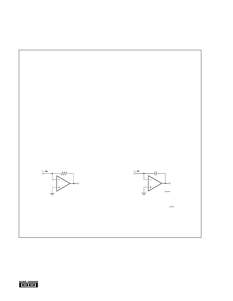
COMPARISON TO CONVENTIONAL TRANSIMPEDANCE AMPLIFIERS
With the conventional transimpedance amplifier circuit
of Figure 2a, input current flows through the feedback
resistor, R
F
, to create a proportional output voltage.
V
O
= –I
IN
R
F
The transimpedance gain is determined by R
F
. Very large
values of R
F
are required to measure very small signal
current. Feedback resistor values exceeding 100M
are
common.
The IVC102 (Figure 2b) provides a similar function,
converting an input current to an output voltage. The
input current flows through the feedback capacitor, C
INT
,
charging it at a rate that is proportional to the input
current. With a constant input current, the IVC102’s
output voltage is
V
O
= –I
IN
T
INT
/C
INT
after an integration time of T
INT
.
V
O
is proportional to the integration time, T
INT
, and
inversely proportional to the feedback capacitor, C
INT
.
The effective transimpedance gain is T
INT
/C
INT
. Ex-
tremely high gain that would be impractical to achieve
with a conventional transimpedance amplifier can be
achieved with small integration capacitor values and/or
long integration times. For example the IVC102 with
C
INT
= 100pF and T
INT
= 100ms provides an effective
transimpedance of 1G
. A 10nA input current would
produce a 10V output after 100ms integration.
The integrating behavior of the IVC102 reduces noise by
averaging the input noise of the sensor, amplifier, and
external sources.
Conventional Transimpedance Amplifier
Figure 2a
Integrating Transimpedance Amplifier
Figure 2b
R
F
V
O
= –I
IN
R
F
V
O
I
IN
CURRENT-OUTPUT SENSORS
Figure 3 shows a model for many current-output sensors
such as photodiodes and ionization chambers. Sensor output
is a signal-dependent current with a very high source resis-
tance. The output is generally loaded into a low impedance
FIGURE 2. Comparison to a Conventional Transimpedance Amplifier.
so that the terminal voltage is kept very low. Typical sensor
capacitance values range from 10pF to over 100pF. This
capacitance plays a key role in operation of the switched-
input measurement technique (see next section).
Provides time-continuous output
voltage proportional to I
IN
.
Output voltage after integration period is
proportional to average I
IN
throughout
the period.
相關PDF資料 |
PDF描述 |
|---|---|
| IVM-20B-500B | Amplifier. Other |
| IVM-20B-70B | Amplifier. Other |
| IWD1205B | Analog IC |
| IWD1205I | Analog IC |
| IWD1205Z | Analog IC |
相關代理商/技術參數(shù) |
參數(shù)描述 |
|---|---|
| IVC102U | 制造商:Texas Instruments 功能描述:AMP INTEG TRANSIMPEDANCE SOIC14 |
| IVC102U/2K5 | 功能描述:跨阻抗放大器 Prec Swtched Integ Transimpedance RoHS:否 制造商:Texas Instruments 封裝 / 箱體:SOIC-14 帶寬:3 MHz 工作電源電壓:36 V 電源電流:5.5 mA 工作溫度范圍:- 40 C to + 85 C 封裝:Tube |
| IVC102U/2K5G4 | 功能描述:跨阻抗放大器 Prec Swtched Integ Transimpedance RoHS:否 制造商:Texas Instruments 封裝 / 箱體:SOIC-14 帶寬:3 MHz 工作電源電壓:36 V 電源電流:5.5 mA 工作溫度范圍:- 40 C to + 85 C 封裝:Tube |
| IVC222HPII | 功能描述:CALIBRATOR CURRENT/VOLTAGE RoHS:是 類別:測試設備 >> 萬用表 - 專用 系列:- 產品目錄繪圖:830B, 890B 標準包裝:1 系列:890 工具類型:電容測試器 適用于相關產品:- 相關產品:LC-29B-ND - CARRY CASE FOR HANDHELD DMM 其它名稱:BK890B |
| IVC-26 | 制造商:PUI Audio 功能描述:INDICATOR VOLUME CONTROL - Bulk |
發(fā)布緊急采購,3分鐘左右您將得到回復。