- 您現(xiàn)在的位置:買賣IC網(wǎng) > PDF目錄22067 > ISPLSI 1016-60LT44I (Lattice Semiconductor Corporation)IC PLD ISP 32I/O 20NS 44TQFP PDF資料下載
參數(shù)資料
| 型號(hào): | ISPLSI 1016-60LT44I |
| 廠商: | Lattice Semiconductor Corporation |
| 文件頁(yè)數(shù): | 15/17頁(yè) |
| 文件大?。?/td> | 0K |
| 描述: | IC PLD ISP 32I/O 20NS 44TQFP |
| 標(biāo)準(zhǔn)包裝: | 160 |
| 系列: | ispLSI® 1000 |
| 可編程類型: | 系統(tǒng)內(nèi)可編程 |
| 最大延遲時(shí)間 tpd(1): | 20.0ns |
| 電壓電源 - 內(nèi)部: | 4.5 V ~ 5.5 V |
| 邏輯元件/邏輯塊數(shù)目: | 16 |
| 門數(shù): | 2000 |
| 輸入/輸出數(shù): | 32 |
| 工作溫度: | -40°C ~ 85°C |
| 安裝類型: | 表面貼裝 |
| 封裝/外殼: | 44-TQFP |
| 供應(yīng)商設(shè)備封裝: | 44-TQFP(10x10) |
| 包裝: | 托盤 |
| 其它名稱: | ISPLSI1016-60LT44I |
第1頁(yè)第2頁(yè)第3頁(yè)第4頁(yè)第5頁(yè)第6頁(yè)第7頁(yè)第8頁(yè)第9頁(yè)第10頁(yè)第11頁(yè)第12頁(yè)第13頁(yè)第14頁(yè)當(dāng)前第15頁(yè)第16頁(yè)第17頁(yè)
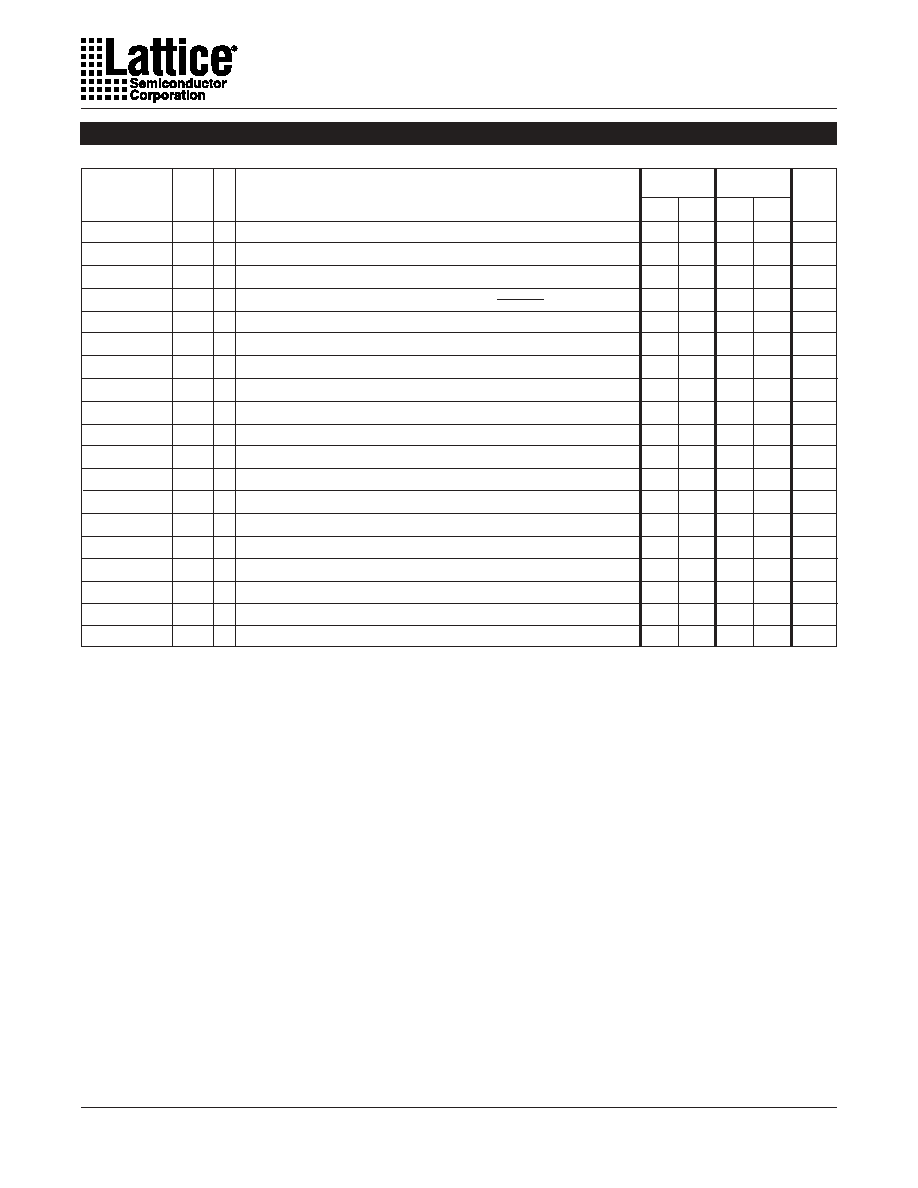
Specifications ispLSI 1016
6
MIN. MAX.
Data Propagation Delay, 4PT bypass, ORP bypass
Data Propagation Delay, Worst Case Path
Clock Frequency with Internal Feedback3
Clock Frequency with External Feedback
Clock Frequency, Max Toggle4
GLB Reg. Setup Time before Clock, 4PT bypass
GLB Reg. Clock to Output Delay, ORP bypass
GLB Reg. Hold Time after Clock, 4 PT bypass
GLB Reg. Setup Time before Clock
GLB Reg. Clock to Output Delay
GLB Reg. Hold Time after Clock
Ext. Reset Pin to Output Delay
Ext. Reset Pulse Duration
Input to Output Enable
Input to Output Disable
Ext. Sync. Clock Pulse Duration, High
Ext. Sync. Clock Pulse Duration, Low
I/O Reg. Setup Time before Ext. Sync. Clock (Y1, Y2)
I/O Reg. Hold Time after Ext. Sync. Clock (Y1, Y2)
ns
MHz
ns
tpd1
tpd2
fmax (Int.)
fmax (Ext.)
fmax (Tog.)
tsu1
tco1
th1
tsu2
tco2
th2
tr1
trw1
ten
tdis
twh
twl
tsu5
th5
1
2
3
4
5
6
7
8
9
10
11
12
13
14
15
16
17
18
19
A
–
A
–
A
–
B
C
–
DESCRIPTION1
PARAMETER
#
2
UNITS
TEST 5
COND.
1
tsu2 + tco1
(
)
MIN. MAX.
–
80
50
100
7
–
0
10
–
0
–
10
–
5
2
6.5
15
20
–
10
–
12
–
17
–
18
–
60
38
83
9
–
0
13
–
0
–
13
–
6
2.5
8.5
20
25
–
13
–
16
–
22.5
–
24
–
-80
-60
Table 2-0030-16/80,60C
1. Unless noted otherwise, all parameters use a GRP load of 4 GLBs, 20 PTXOR path, ORP and Y0 clock.
2. Refer to Timing Model in this data sheet for further details.
3. Standard 16-Bit loadable counter using GRP feedback.
4. fmax (Toggle) may be less than 1/(twh + twl). This is to allow for a clock duty cycle of other than 50%.
5. Reference Switching Test Conditions Section.
External Timing Parameters
Over Recommended Operating Conditions
ALL
DEVICES
DISCONTINUED
相關(guān)PDF資料 |
PDF描述 |
|---|---|
| ISL61862FIRZ-T | IC USB PWR CTRLR 1.5A 8DFN |
| VI-270-CY-F2 | CONVERTER MOD DC/DC 5V 50W |
| THJB106M016RJN | CAP TANT 10UF 16V 20% 1210 |
| TRJB156M020RRJ | CAP TANT 15UF 20V 20% 1210 |
| ISL61862CIRZ-T | IC USB PWR CTRLR 3A 8DFN |
相關(guān)代理商/技術(shù)參數(shù) |
參數(shù)描述 |
|---|---|
| ispLSI1016-60LT44I | 功能描述:CPLD - 復(fù)雜可編程邏輯器件 USE ispMACH 4000V RoHS:否 制造商:Lattice 系列: 存儲(chǔ)類型:EEPROM 大電池?cái)?shù)量:128 最大工作頻率:333 MHz 延遲時(shí)間:2.7 ns 可編程輸入/輸出端數(shù)量:64 工作電源電壓:3.3 V 最大工作溫度:+ 90 C 最小工作溫度:0 C 封裝 / 箱體:TQFP-100 |
| ispLSI1016-80LJ | 功能描述:CPLD - 復(fù)雜可編程邏輯器件 USE ispMACH 4000V RoHS:否 制造商:Lattice 系列: 存儲(chǔ)類型:EEPROM 大電池?cái)?shù)量:128 最大工作頻率:333 MHz 延遲時(shí)間:2.7 ns 可編程輸入/輸出端數(shù)量:64 工作電源電壓:3.3 V 最大工作溫度:+ 90 C 最小工作溫度:0 C 封裝 / 箱體:TQFP-100 |
| ISPLSI1016-80LT | 制造商:未知廠家 制造商全稱:未知廠家 功能描述:Electrically-Erasable Complex PLD |
| ispLSI1016-80LT44 | 功能描述:CPLD - 復(fù)雜可編程邏輯器件 USE ispMACH 4000V RoHS:否 制造商:Lattice 系列: 存儲(chǔ)類型:EEPROM 大電池?cái)?shù)量:128 最大工作頻率:333 MHz 延遲時(shí)間:2.7 ns 可編程輸入/輸出端數(shù)量:64 工作電源電壓:3.3 V 最大工作溫度:+ 90 C 最小工作溫度:0 C 封裝 / 箱體:TQFP-100 |
| ispLSI1016-90LJ | 功能描述:CPLD - 復(fù)雜可編程邏輯器件 USE ispMACH 4000V RoHS:否 制造商:Lattice 系列: 存儲(chǔ)類型:EEPROM 大電池?cái)?shù)量:128 最大工作頻率:333 MHz 延遲時(shí)間:2.7 ns 可編程輸入/輸出端數(shù)量:64 工作電源電壓:3.3 V 最大工作溫度:+ 90 C 最小工作溫度:0 C 封裝 / 箱體:TQFP-100 |
發(fā)布緊急采購(gòu),3分鐘左右您將得到回復(fù)。