- 您現(xiàn)在的位置:買賣IC網(wǎng) > PDF目錄360996 > ISO106 SIGNAL ISOLATION BUFFER AMPLIFIERS PDF資料下載
參數(shù)資料
| 型號(hào): | ISO106 |
| 英文描述: | SIGNAL ISOLATION BUFFER AMPLIFIERS |
| 中文描述: | 信號(hào)隔離緩沖放大器 |
| 文件頁(yè)數(shù): | 9/15頁(yè) |
| 文件大小: | 230K |
| 代理商: | ISO106 |
第1頁(yè)第2頁(yè)第3頁(yè)第4頁(yè)第5頁(yè)第6頁(yè)第7頁(yè)第8頁(yè)當(dāng)前第9頁(yè)第10頁(yè)第11頁(yè)第12頁(yè)第13頁(yè)第14頁(yè)第15頁(yè)
9
ISO102/106
noise power varies with the square root of the bandwidth of
the buffer. It is recommended that the bandwidth be reduced
to about twice the maximum signal bandwidth for optimum
dynamic range as shown in the “Dynamic Range vs Band-
width” performance curve. The output spectral noise density
measurement is displayed in the “Output Spectral Noise
Density” performance curve. The noise is flat to within
5dB
√
Hz between 0.1Hz to 70kHz.
The overall AC gain of the buffer amplifiers is shown in two
performance curves: “Gain Flatness vs Frequency” and
“Gain/Phase vs Frequency.” Note that with C
1
= 100pF and
C
= 200pF, the AC gain remains flat within
±
0.01dB up to
7kHz. The total harmonic distortion for large-signal sine
wave outputs is plotted in the “Total Harmonic Distortion”
performance curve. The phase-lock-loop displays slightly
nonuniform rise and fall edges under maximum slew condi-
tions. Reducing the output filter bandwidth to below 70kHz
smoothes the output signal and eliminates any overshoot.
See the “Large Signal Transient Response” performance
curve.
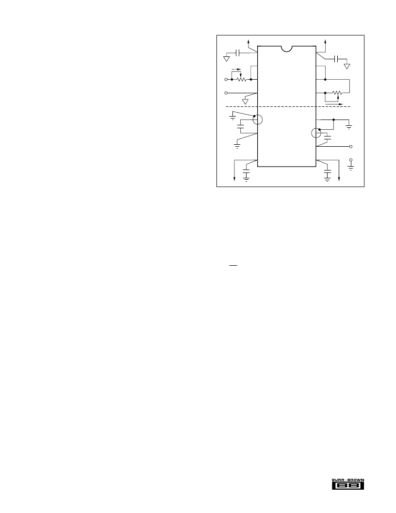
OPTIONAL OFFSET AND GAIN ADJUSTMENT
In many applications the factory-trimmed offset is adequate.
For situations where reduced or modified gain and offset are
required, adjustment of each is easy. The addition of two
potentiometers as shown in Figure 4 provides for a two step
calibration.
Offset should be adjusted first. Gain adjustment does not
interfere with offset. The potentiometer’s TCR adds only
2% to overall temperature drift. The offset and gain adjust-
ment procedures are as follows:
1. Set V
IN
to 0V and adjust R
1
to desired offset at the output.
2. Set V
IN
to full scale (not zero). Adjust R
2
for desired gain.
ISOLATION-MODE REJECTION
The IS0102 and IS0106 provide exceptionally high isola-
tion-mode rejection over a wide range of isolation-mode
voltages and frequencies. The typical performance curves
should be used to insure operation within the recommended
range. The maximum barrier voltage allowed decreases as
the frequency of the voltage increases. As with all isolation
amplifiers, a change of voltage across the barrier will induce
leakage current across the barrier. In the case of the IS0102
and IS0106, there exists a threshold of leakage current
through the signal capacitors that can cause over-drive of the
decoder’s sense amplifier. This occurs when the slew rate of
the isolation voltage reaches 100V/
μ
s. The output will
recover in about 50
μ
s from transients exceeding 100V/
μ
s.
The first two performance curves indicate the expected
isolation-mode rejection over a wide range of isolation
voltage frequencies. Also plotted is the typical leakage
current across the barrier at 240Vrms. The majority of the
leakage current is between the input common pin and the
output digital ground pin.
The IS0102 and IS0106 are intended to be continuously
operated with fully rated isolation voltage and temperature
without significant drift of gain and offset. See the “Gain
Error/Offset Isolation Voltage” performance curve for
changes in gain and offset with isolation voltage.
SUPPLY AND TEMPERATURE RANGE
The IS0102 and IS0106 are rated for +15V supplies; how-
ever, they are guaranteed to operate from
±
10V to
±
20V.
Performance is also rated for an ambient temperature range
of –25
°
C to +85
°
C. For operation outside this temperature
range, refer to the “Power Dissipation vs Temperature”
performance curve to establish the maximum allowed sup-
ply voltage. Supply currents are fairly insensitive to changes
in supply voltage or temperature. Therefore, the maximum
current limits can be used in computing the maximum
junction temperature under nonrated conditions.
OPTIONAL BANDWIDTH CONTROL
The following discussion relates optimum dynamic range
performance to bandwidth, noise, and settling time.
The outputs of the IS0102 and IS0106 are the outputs of a
second-order low-pass Butterworth filter. Its low impedance
output is rated for
±
5mA drive and
±
12V range with 10,000pF
loads. The closed-loop bandwidth of the PLL is 70kHz,
while the output filter is internally set at 100kHz. The output
filter lowers the residual voltage of the barrier FM signal to
below the noise floor of the output signal.
Two pins are available for optional modification of the
filter’s bandwidth. Only two capacitors are required. The
“Bandwidth Control” performance curve gives the value of
C
(C
is equal to twice C
) for the desired bandwidth. Figure
4 illustrates the optional connection of both capacitors.
A tradeoff can be achieved between the required signal
bandwidth and system dynamic range. The noise floor of the
output limits the dynamic range of the output signal. The
–V
V
Gain Adjust
Common
IN
CC1
1
Common
Reference
+V
2
CC2
2
Digital Common
V
–V
+V
Offset Adjust
Offset
Reference
1
0.1μF
IN
V
0.1μF
0.1μF
0.1μF
OUT
V
ISO102/106
NC
–15V
2
C
2
R
1k
+15V
–15V
1
R
5k
C
1
+15V
Increase
Offset
Increase Gain
* PCB rings terminate HV fields.
C
1
2
C
*
*
FIGURE 4. Optional Gain Adjust, Offset Adjust, and Band-
width Control.
相關(guān)PDF資料 |
PDF描述 |
|---|---|
| ISO106B | SIGNAL ISOLATION BUFFER AMPLIFIERS |
| ISO102 | SIGNAL ISOLATION BUFFER AMPLIFIERS |
| ISO103 | Low-Cost, Internally Powered ISOLATION AMPLIFIER |
| ISO103B | Low-Cost, Internally Powered ISOLATION AMPLIFIER |
| ISO107 | High-Voltage, Internally Powered ISOLATION AMPLIFIER |
相關(guān)代理商/技術(shù)參數(shù) |
參數(shù)描述 |
|---|---|
| ISO106B | 功能描述:隔離放大器 Wide BW Std Hermetic Sig Iso Buffer Amp RoHS:否 制造商:Texas Instruments 輸入補(bǔ)償電壓:1.5 mV 共模抑制比(最小值):95 dB 帶寬:60 KHz 工作電源電壓:3.3 V 電源電流:8 mA 工作溫度范圍:- 40 C to + 105 C 安裝風(fēng)格:SMD/SMT 封裝 / 箱體:SOP-8 封裝:Tube |
| ISO107 | 功能描述:特殊用途放大器 Hi-Vltg Internally Pwrd Iso Amp RoHS:否 制造商:Texas Instruments 通道數(shù)量:Single 共模抑制比(最小值): 輸入補(bǔ)償電壓: 工作電源電壓:3 V to 5.5 V 電源電流:5 mA 最大功率耗散: 最大工作溫度:+ 70 C 最小工作溫度:- 40 C 安裝風(fēng)格:SMD/SMT 封裝 / 箱體:QFN-20 封裝:Reel |
| ISO113 | 功能描述:隔離器接口集成電路 Lo-Cost Hi Vltg Iso Amp RoHS:否 制造商:Texas Instruments 通道數(shù)量:2 傳播延遲時(shí)間: 電源電壓-最大:5.5 V 電源電壓-最小:3 V 電源電流:3.6 mA 功率耗散: 最大工作溫度:+ 125 C 安裝風(fēng)格: 封裝 / 箱體:SOIC-8 封裝:Tube |
| ISO113B | 功能描述:隔離器接口集成電路 Lo-Cost Hi Vltg Iso Amp RoHS:否 制造商:Texas Instruments 通道數(shù)量:2 傳播延遲時(shí)間: 電源電壓-最大:5.5 V 電源電壓-最小:3 V 電源電流:3.6 mA 功率耗散: 最大工作溫度:+ 125 C 安裝風(fēng)格: 封裝 / 箱體:SOIC-8 封裝:Tube |
| ISO1176 | 制造商:TI 制造商全稱:Texas Instruments 功能描述:ISOLATED RS-485 PROFIBUS TRANSCEIVER |
發(fā)布緊急采購(gòu),3分鐘左右您將得到回復(fù)。