- 您現(xiàn)在的位置:買賣IC網(wǎng) > PDF目錄2081 > ISL45041IRZ-T (Intersil)IC VCOM CALIBRATOR TFT/LCD 8TDFN PDF資料下載
參數(shù)資料
| 型號: | ISL45041IRZ-T |
| 廠商: | Intersil |
| 文件頁數(shù): | 4/7頁 |
| 文件大?。?/td> | 0K |
| 描述: | IC VCOM CALIBRATOR TFT/LCD 8TDFN |
| 標(biāo)準(zhǔn)包裝: | 6,000 |
| 類型: | 校準(zhǔn)器 |
| 應(yīng)用: | LCD 顯示器 |
| 安裝類型: | 表面貼裝 |
| 封裝/外殼: | 8-WDFN 裸露焊盤 |
| 供應(yīng)商設(shè)備封裝: | 8-TDFN(3x3) |
| 包裝: | 帶卷 (TR) |

4
All Intersil U.S. products are manufactured, assembled and tested utilizing ISO9000 quality systems.
Intersil Corporation’s quality certifications can be viewed at www.intersil.com/design/quality
Intersil products are sold by description only. Intersil Corporation reserves the right to make changes in circuit design, software and/or specifications at any time without
notice. Accordingly, the reader is cautioned to verify that data sheets are current before placing orders. Information furnished by Intersil is believed to be accurate and
reliable. However, no responsibility is assumed by Intersil or its subsidiaries for its use; nor for any infringements of patents or other rights of third parties which may result
from its use. No license is granted by implication or otherwise under any patent or patent rights of Intersil or its subsidiaries.
For information regarding Intersil Corporation and its products, see www.intersil.com
FN6189.4
December 17, 2010
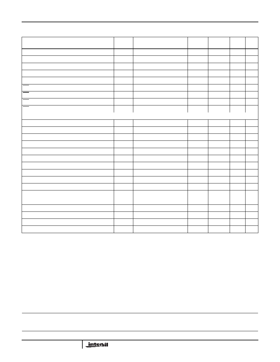
SDA, SCL Input Logic High
I2CVIH
0.7*VDD
V
SDA, SCL Input Logic Low
I2CVIL
0.55
V
SDA, SCL Hysteresis
(Note 9)
260
mV
SDA Output Logic High
VOHS
VDD - 0.4
V
SDA Output Logic Low
VOLS
@ 3mA
0.4
V
WP Input Logic High
VIH
0.7*VDD
V
WP Input Logic Low
VIL
0.3*VDD
V
WP Hysteresis
(Note 9)
0.14VDD
V
WP Input Current
ILWPN
0.20
35
A
I2C Timing
SCL Clock Frequency
fSCL
0
400
kHz
I2C Clock High Time
tSCH
0.6
s
I2C Clock Low Time
tSCL
1.3
s
I2C Spike Rejection Filter Pulse Width
tDSP
050
ns
I2C Data Set Up Time
tSDS
100
ns
I2C Data Hold Time
tSDH
900
ns
I2C SDA, SCL Input Rise Time
tICR
Dependent on Load (Note 10)
20 + 0.1*Cb
1000
ns
I2C SDA, SCL Input Fall Time
tICF
(Note 10)
20 + 0.1*Cb
300
ns
I2C Bus Free Time Between Stop and Start
tBUF
200
s
I2C Repeated Start Condition Set-up
tSTS
0.6
s
I2C Repeated Start Condition Hold
tSTH
0.6
s
I2C Stop Condition Set-up
tSPS
0.6
s
I2C Bus Capacitive Load
Cb
400
pF
SDA Pin Capacitance
CSDA
10
pF
SCL Pin Capacitance
CS
10
pF
EEPROM Write Cycle Time
tW
100
ms
NOTES:
6. Compliance to datasheet limits is assured by one or more methods: production test, characterization and/or design.
7. IDD current may increase to 2mA for 45ms or less during each EEPROM programming operation.
8. IAVDD current may increase to 1mA for 30ms or less during each EEPROM programming operation.
9. Simulated and Determined via Design and NOT Directly Tested.
10. Simulated and Designed According to I2C Specifications.
11. A typical Current of 20
12. Minimum value of RSET resistor guaranteed when: AVDD = 15V, VDD = 3.0V and when voltage on the VOUT pin is greater than 2.5V. Reference
Electrical Specifications
Test Conditions: VDD = 3.3V, AVDD = 18V, RSET = 5k, R1 = 10k, R2 = 10k; (See Figure 1) Unless
Otherwise Specified. Typicals are at TA = +25°C. Boldface limits apply over the operating temperature range, 0°C to +85°C. (Continued)
PARAMETER
SYMBOL
TEST CONDITIONS
MIN
(Note 6)
TYP
MAX
(Note 6) UNITS
ISL45041
相關(guān)PDF資料 |
PDF描述 |
|---|---|
| ISL45042AIRZ-T | IC LCD CALIBRATOR 8-TDFN |
| ISL45042IR-T | IC LCD MODULE CALIBRATOR 8-DFN |
| ISL54002IRTZ | IC AMP AUDIO PWR 1.23W AB 20TQFN |
| ISL54004IRTZ-T | IC AMP AUDIO PWR 1.23W AB 20TQFN |
| ISL54006IRTZ | IC AMP AUDIO PWR 1.23W AB 20TQFN |
相關(guān)代理商/技術(shù)參數(shù) |
參數(shù)描述 |
|---|---|
| ISL45042 | 制造商:INTERSIL 制造商全稱:Intersil Corporation 功能描述:LCD Module Calibrator |
| ISL45042_06 | 制造商:INTERSIL 制造商全稱:Intersil Corporation 功能描述:LCD Module Calibrator |
| ISL45042_07 | 制造商:INTERSIL 制造商全稱:Intersil Corporation 功能描述:LCD Module Calibrator |
| ISL45042_11 | 制造商:INTERSIL 制造商全稱:Intersil Corporation 功能描述:LCD Module Calibrator |
| ISL45042A | 制造商:INTERSIL 制造商全稱:Intersil Corporation 功能描述:LCD Module Calibrator |
發(fā)布緊急采購,3分鐘左右您將得到回復(fù)。