- 您現(xiàn)在的位置:買賣IC網(wǎng) > PDF目錄377537 > IRPT1059 (International Rectifier) Intergrated Power Stage for 0.75kW Motor Drives(0.75kW 馬達驅(qū)動器的集成功率單元) PDF資料下載
參數(shù)資料
| 型號: | IRPT1059 |
| 廠商: | International Rectifier |
| 英文描述: | Intergrated Power Stage for 0.75kW Motor Drives(0.75kW 馬達驅(qū)動器的集成功率單元) |
| 中文描述: | 集成功率級的功率0.75kW電動機驅(qū)動器(功率0.75kW馬達驅(qū)動器的集成功率單元) |
| 文件頁數(shù): | 3/12頁 |
| 文件大?。?/td> | 333K |
| 代理商: | IRPT1059 |
IRPT1059
www.irf.com
page 3
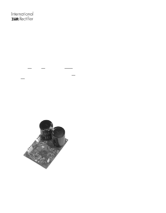
Figure 3. IRPT1059D Driver-PlusBoard
The
protection circuitry
receives current signals from shunts
in positive and negative DC bus rail for
earth/ground fault
and
short-circuit
conditions.
Any earth-fault signal is fed through an
opto-isolator to the protection circuitry.
Current signal from
negative DC bus rail is provided on the J3 connector as
current
feedback
, IFB (0.045V/A).
If filtering of this signal is required,
it should be done by adding a high-impedance buffer stage
between signal and filter.
DC bus voltage is scaled down
to
provided a voltage signal on the J3 connector as
voltage
feedback
, VFB (0.023 x Bus voltage).
Thermal sense signal for
over-temperature
protection is obtained from a thermistor
housed inside the power module.
The thermistor activates the
latch if the temperature of the power module’s
IMS substrate
exceeds a set level.
The system is designed for 150% overload for one minute
while operating with the specified heat sink.
The external
microcontroller should shut off PWM signals if the overload
condition persists for more than one minute.
The
switching power supply
employs the IR2152S
self-
oscillating driver chip in a buck regulator topology to deliver
nominal 15V and 5V DC outputs,
referenced to the negative DC
bus (N).
The power supply
feeds the gate drive and protection
circuits.
The 15V and 5V outputs are available on the
control
interface connector’s
(J3) VCC and VDD pins for external
microprocessor and control logic supply.
The IRPT1059D Driver-Plus Board
The IRPT1059D Driver-
Plus
board, shown in figure 3, houses
surge suppression MOV on input, a switching power supply, a DC
bus filter capacitor with NTC inrush current limiter, an IR2132J
monolithic
3-phase driver IC,
and protection and sensing circuitry.
The inverter
gate drive circuit
, implemented with an IR2132J
monolithic 3-phase HVIC driver, delivers
on/off gate drive
signals to the IGBTs’ gates, corresponding with input PWM
control signals IN1 through IN6.
After power-up, RESET pin on
the J3 connector must be held low (with open collector
configuration) for at least 2
μ
sec while all PWM signals, IN1
through IN6 are held high (off condition). A latch in the
protection circuitry is set high during a fault condition to trip the
IR2132J’s internal latch and shut down all PWM output gate
drive signals and cause the FAULT output pin on IR2132J to set
low and light the LED.
The Fault diagnostic is an active low,
open drain output
with a pull-up resistor.
This signal is provided
on the J3 connector for
fault
feedback to external control logic.
相關(guān)PDF資料 |
PDF描述 |
|---|---|
| IRPT1059D | Integrated Power Stage for 1hp Motor Drives |
| IRPT1059E | Integrated Power Stage for 1hp Motor Drives |
| IRPT1060C | nullIntegrated Power Stage for 1 hp Motor Drives |
| IRPT1061 | Intergrated Power Stage for 0.75kW Motor Drives(0.75kW 馬達驅(qū)動器的集成功率單元) |
| IRPT1060D | nullIntegrated Power Stage for 1 hp Motor Drives |
相關(guān)代理商/技術(shù)參數(shù) |
參數(shù)描述 |
|---|---|
| IRPT1059A | 制造商:IRF 制造商全稱:International Rectifier 功能描述:Integrated Power Stage for 1hp Motor Drives |
| IRPT1059C | 制造商:IRF 制造商全稱:International Rectifier 功能描述:Integrated Power Stage for 1hp Motor Drives |
| IRPT1059D | 制造商:IRF 制造商全稱:International Rectifier 功能描述:Integrated Power Stage for 1hp Motor Drives |
| IRPT1059E | 制造商:IRF 制造商全稱:International Rectifier 功能描述:Integrated Power Stage for 1hp Motor Drives |
| IRPT1060 | 制造商:IRF 制造商全稱:International Rectifier 功能描述:nullIntegrated Power Stage for 1 hp Motor Drives |
發(fā)布緊急采購,3分鐘左右您將得到回復。