- 您現在的位置:買賣IC網 > PDF目錄377520 > IRGPC40MD2 (International Rectifier) Insulated Gate Bipolar Transistors (IGBTs)(短路額定快速絕緣柵型雙極型晶體管) PDF資料下載
參數資料
| 型號: | IRGPC40MD2 |
| 廠商: | International Rectifier |
| 英文描述: | Insulated Gate Bipolar Transistors (IGBTs)(短路額定快速絕緣柵型雙極型晶體管) |
| 中文描述: | 絕緣門雙極晶體管(IGBTs)(短路額定快速絕緣柵型雙極型晶體管) |
| 文件頁數: | 2/2頁 |
| 文件大?。?/td> | 42K |
| 代理商: | IRGPC40MD2 |
C-398
IRGPC40MD2
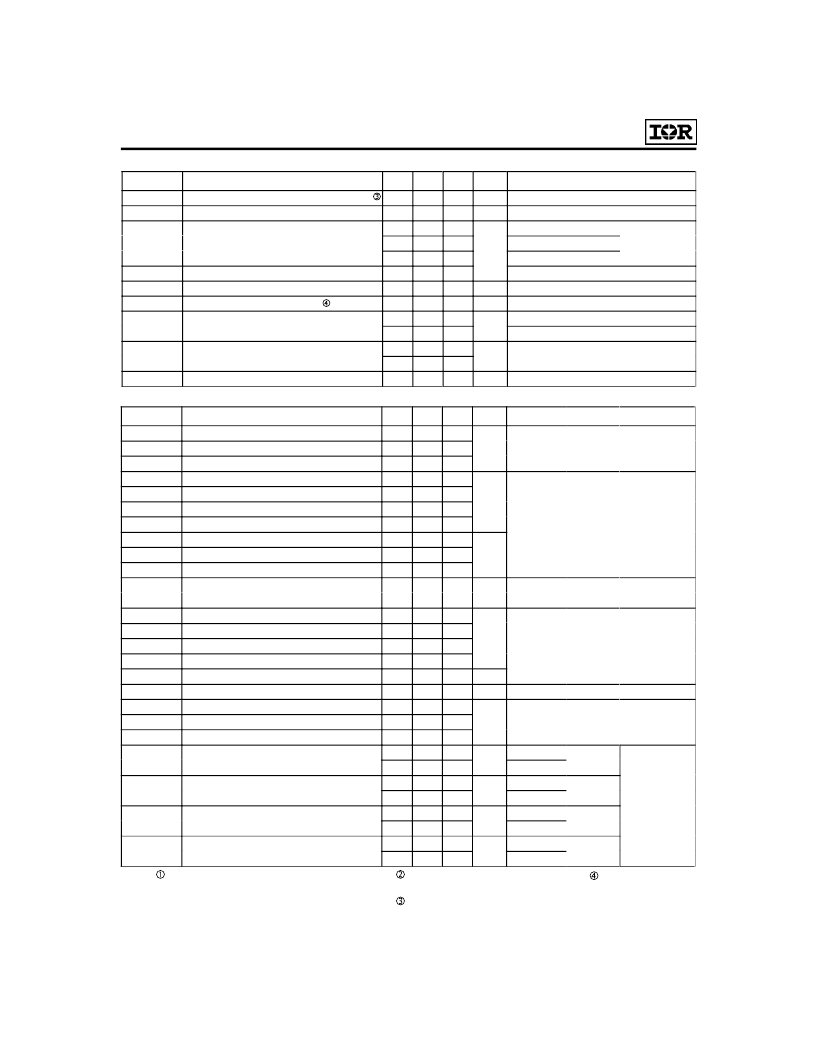
Electrical Characteristics @ T
J
= 25°C (unless otherwise specified)
Parameter
V
(BR)CES
Collector-to-Emitter Breakdown Voltage
V
(BR)CES
/
T
J
Temperature Coeff. of Breakdown Voltage
V
CE(on)
Collector-to-Emitter Saturation Voltage
Min. Typ. Max. Units
600
—
—
0.70
—
2.0
—
2.6
—
2.4
3.0
—
—
-12
9.2
12
—
—
—
—
3500
—
1.3
—
1.2
—
—
±100
Conditions
—
—
3.0
—
—
5.5
—
—
250
V
V
GE
= 0V, I
C
= 250μA
V
GE
= 0V, I
C
= 1.0mA
I
C
= 24A
I
C
= 40A
I
C
= 24A, T
J
= 150°C
V
CE
= V
GE
, I
C
= 250μA
V
CE
= V
GE
, I
C
= 250μA
V
CE
= 100V, I
C
= 24A
V
GE
= 0V, V
CE
= 600V
V
GE
= 0V, V
CE
= 600V, T
J
= 150°C
I
C
= 15A
I
C
= 15A, T
J
= 150°C
V
GE
= ±20V
V/°C
V
GE
= 15V
V
V
GE(th)
V
GE(th)
/
T
J
Temperature Coeff. of Threshold Voltage
g
fe
Forward Transconductance
I
CES
Zero Gate Voltage Collector Current
Gate Threshold Voltage
mV/°C
S
μA
V
FM
Diode Forward Voltage Drop
1.7
1.6
V
I
GES
Switching Characteristics @ T
J
= 25°C (unless otherwise specified)
Parameter
Q
g
Total Gate Charge (turn-on)
Qge
Gate - Emitter Charge (turn-on)
Q
gc
Gate - Collector Charge (turn-on)
t
d(on)
Turn-On Delay Time
t
r
Rise Time
t
d(off)
Turn-Off Delay Time
t
f
Fall Time
E
on
Turn-On Switching Loss
E
off
Turn-Off Switching Loss
E
ts
Total Switching Loss
t
sc
Short Circuit Withstand Time
Gate-to-Emitter Leakage Current
nA
Min. Typ. Max. Units
—
59
—
8.6
—
25
—
26
—
37
—
240
—
230
—
0.75
—
1.65
—
2.4
10
—
Conditions
80
10
42
—
—
410
420
—
—
3.6
—
I
C
= 24A
V
CC
= 400V
nC
T
J
= 25°C
I
C
= 24A, V
CC
= 480V
V
GE
= 15V, R
G
Energy losses include "tail" and
diode reverse recovery.
ns
mJ
μs
V
CC
= 360V, T
J
= 125°C
V
GE
= 15V, R
G
= 10
, V
CPK
< 500V
T
J
= 150°C,
I
C
= 24A, V
CC
= 480V
V
GE
= 15V, R
G
= 10
Energy losses include "tail" and
diode reverse recovery.
Measured 5mm from package
V
GE
= 0V
V
CC
= 30V
= 1.0MHz
T
J
= 25°C
T
J
= 125°C
T
J
= 25°C
T
J
= 125°C
T
J
= 25°C
T
J
= 125°C
T
J
= 25°C
T
J
= 125°C
t
d(on)
t
r
t
d(off)
t
f
E
ts
L
E
C
ies
C
oes
C
res
t
rr
Turn-On Delay Time
Rise Time
Turn-Off Delay Time
Fall Time
Total Switching Loss
Internal Emitter Inductance
Input Capacitance
Output Capacitance
Reverse Transfer Capacitance
Diode Reverse Recovery Time
—
—
—
—
—
—
—
—
—
—
—
—
—
—
—
—
—
28
37
380
460
4.5
13
1500
190
20
42
74
4.0
6.5
80
220
188
160
V
CC
=80%(V
CES
), V
GE
=20V, L=10μH,
R
G
= 10
.
Pulse width
≤
80μs; duty factor
≤
0.1%.
—
—
—
—
—
—
—
—
—
60
120
6.0
10
180
600
—
—
ns
mJ
nH
pF
ns
I
F
= 15A
I
rr
Diode Peak Reverse Recovery Current
A
V
R
= 200V
Q
rr
Diode Reverse Recovery Charge
nC
di/dt = 200A/μs
di
(rec)M
/dt
Diode Peak Rate of Fall of Recovery
During t
b
Repetitive rating; V
GE
=20V, pulse width limited
by max. junction temperature.
Refer to Section D for the following:
Package Outline 3
- JEDEC Outline TO-247AC
A/μs
Notes:
Pulse width 5.0μs,
single shot.
Section D - page D-13
相關PDF資料 |
PDF描述 |
|---|---|
| IRGPC40M | Insulated Gate Bipolar Transistors (IGBTs)(短路額定快速絕緣柵型雙極型晶體管) |
| IRGPC40U | Insulated Gate Bipolar Transistors (IGBTs)(超快速絕緣柵型雙極型晶體管) |
| IRGPC50KD2 | INSULATED GATE BIPOLAR TRANSISTOR WITH ULTRAFAST SOFT RECOVERY DIODE |
| IRGPC50FD2 | INSULATED GATE BIPOLAR TRANSISTOR WITH ULTRAFAST SOFT RECOVERY(Vces=600V, @Vge=15V,Ic=39A) |
| IRGPC50UD2 | 320 x 240 pixel format, LED or CFL Backlight |
相關代理商/技術參數 |
參數描述 |
|---|---|
| IRGPC40S | 制造商:IRF 制造商全稱:International Rectifier 功能描述:Fit Rate / Equivalent Device Hours |
| IRGPC40U | 制造商:IRF 制造商全稱:International Rectifier 功能描述:Fit Rate / Equivalent Device Hours |
| IRGPC40UD2 | 制造商:IRF 制造商全稱:International Rectifier 功能描述:INSULATED GATE BIPOLAR TRANSISTOR WITH ULTRAFAST SOFT RECOVERY DIODE(Vces=600V, @Vge=15V, Ic=20A) |
| IRGPC46 | 制造商:未知廠家 制造商全稱:未知廠家 功能描述:TRANSISTOR | IGBT | N-CHAN | 600V V(BR)CES | 60A I(C) | TO-247AC |
| IRGPC50 | 制造商:未知廠家 制造商全稱:未知廠家 功能描述:TRANSISTOR | IGBT | N-CHAN | 600V V(BR)CES | 55A I(C) | TO-247AC |
發(fā)布緊急采購,3分鐘左右您將得到回復。