- 您現(xiàn)在的位置:買(mǎi)賣(mài)IC網(wǎng) > PDF目錄383117 > IRF9233 (HARRIS SEMICONDUCTOR) CAP CER 250VAC 330PF X7R 1808 PDF資料下載
參數(shù)資料
| 型號(hào): | IRF9233 |
| 廠商: | HARRIS SEMICONDUCTOR |
| 元件分類: | 功率晶體管 |
| 英文描述: | CAP CER 250VAC 330PF X7R 1808 |
| 中文描述: | 5.5 A, 150 V, 1.2 ohm, P-CHANNEL, Si, POWER, MOSFET, TO-204AA |
| 文件頁(yè)數(shù): | 2/7頁(yè) |
| 文件大小: | 72K |
| 代理商: | IRF9233 |
6-2
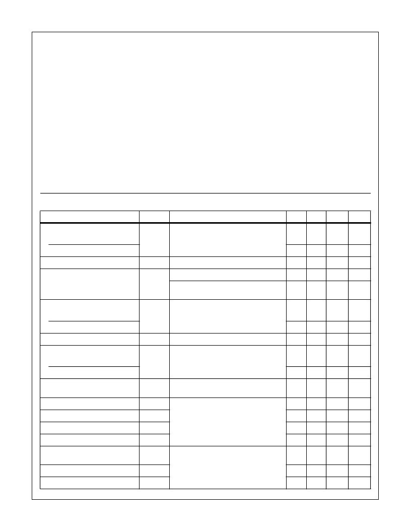
Absolute Maximum Ratings
T
C
= 25
o
C, Unless Otherwise Specified
IRF9230
-200
-200
-6.5
-4.0
-26
±
20
75
0.6
500
-55 to 150
IRF9231
-150
-150
-6.5
-4.0
-26
±
20
75
0.6
500
-55 to 150
IRF9232
-200
-200
-5.5
-3.5
-22
±
20
75
0.6
500
-55 to 150
IRF9233
-150
-150
-5.5
-3.5
-22
±
20
75
0.6
500
-55 to 150
UNITS
V
V
A
A
A
V
W
W/
o
C
mJ
o
C
Drain to Source Breakdown Voltage (Note 1). . . . . . . . . . . V
DS
Drain to Gate Voltage (R
GS
= 20k
)
(Note 1) . . . . . V
DGRVGS
Continuous Drain Current. . . . . . . . . . . . . . . . . . . . . . . . . . . . I
D
T
C
= 100
o
C. . . . . . . . . . . . . . . . . . . . . . . . . . . . . . . . . . . . . I
D
Pulsed Drain Current (Note 3) . . . . . . . . . . . . . . . . . . . . . . .I
DM
Gate to Source Voltage . . . . . . . . . . . . . . . . . . . . . . . . . . . V
GS
Maximum Power Dissipation . . . . . . . . . . . . . . . . . . . . . . . . P
D
Linear Derating Factor . . . . . . . . . . . . . . . . . . . . . . . . . . . . . .
Single Pulse Avalanche Energy Rating (Note 4) . . . . . . . . . . E
AS
Operating and Storage Temperature . . . . . . . . . . . . . T
J,
T
STG
Maximum Temperature for Soldering
Leads at 0.063in (1.6mm) from Case for 10s . . . . . . . . . . .T
L
Package Body for 10s, See Techbrief 334 . . . . . . . . . . . T
pkg
CAUTION: Stresses above those listed in “Absolute Maximum Ratings” may cause permanent damage to the device. This is a stress only rating and operation
of the device at these or any other conditions above those indicated in the operational sections of this specification is not implied.
300
260
300
260
300
260
300
260
o
C
o
C
NOTE:
1. T
J
= 25
o
C to T
J
= 125
o
C.
Electrical Specifications
T
C
= 25
o
C, Unless Otherwise Specified
PARAMETER
SYMBOL
TEST CONDITIONS
MIN
TYP
MAX
UNITS
Drain to Source Breakdown Voltage
BV
DSS
I
D
= -250
μ
A, V
GS
= 0V, (Figure10)
IRF9230, IRF9232
-200
-
-
V
IRF9231, IRF9233
-150
-
-
V
Gate Threshold Voltage
V
GS(TH)
V
GS
= V
DS
, I
D
= -250
μ
A
-2
-
-4
V
Zero Gate Voltage Drain Current
I
DSS
V
DS
= Rated BV
DSS
, V
GS
= 0V
-
-
-25
μ
A
V
DS
= 0.8 x Rated BV
DSS
, V
GS
= 0V
T
C
= 125
o
C
-
-
-250
μ
A
On-State Drain Current (Note 2)
I
D(ON)
V
DS
> I
D(ON)
x r
DS(ON) MAX
, V
GS
= -10V,
(Figure 7)
IRF9230, IRF9231
-6.5
-
-
A
IRF9232, IRF9233
-5.5
-
-
A
Gate to Source Leakage Current
I
GSS
V
GS
=
±
20V
-
-
±
100
nA
Drain to Source On Resistance (Note 2)
r
DS(ON)
I
D
= -3.5A, V
GS
= -10V, (Figures 8, 9)
IRF9230, IRF9231
-
0.5
0.8
IRF9232, IRF9233
-
0.8
1.2
Forward Transconductance (Note 2)
g
fs
V
DS
> I
D(ON)
x r
DS(ON) MAX
, I
D
= -3.5A,
(Figure 12)
2.2
3.5
-
S
Turn-On Delay Time
t
d(ON)
V
DD
= 0.5 x Rated BV
DSS
, I
D
≈
-6.5A,
R
G
= 50
,
V
GS
=
-
10V, (Figure 17, 18)
R
L
= 14.7
for V
DSS
= 200V
R
L
= 10.9
for V
DSS
= 150V
MOSFET Switching Times are Essentially
Independent of Operating Temperature
-
30
50
ns
Rise Time
t
r
-
50
100
ns
Turn-Off Delay Time
t
d(OFF)
-
50
100
ns
Fall Time
t
f
-
40
80
ns
Total Gate Charge
(Gate to Source + Gate to Drain)
Q
g(TOT)
V
GS
= -10V, I
D
= -6.5A, V
DS
= 0.8 x Rated
BV
DSS,
(Figures 14, 19, 20)
Gate Charge is Essentially Independent
of Operating Temperature
-
31
45
nC
Gate to Source Charge
Q
gs
-
18
-
nC
Gate to Drain “Miller” Charge
Q
gd
-
13
-
nC
IRF9230, IRF9231, IRF9232, IRF9233
相關(guān)PDF資料 |
PDF描述 |
|---|---|
| IRF9231 | -5.5A and -6.5A, -150V and -200V, 0.8 and 1.2 Ohm, P-Channel Power MOSFETs |
| IRF9232 | -5.5A and -6.5A, -150V and -200V, 0.8 and 1.2 Ohm, P-Channel Power MOSFETs |
| IRFC150 | HIGH VOLTAGE POWER MOSFET DIE |
| IRFP152 | HIGH VOLTAGE POWER MOSFET DIE |
| IRFP153 | HIGH VOLTAGE POWER MOSFET DIE |
相關(guān)代理商/技術(shù)參數(shù) |
參數(shù)描述 |
|---|---|
| IRF9240 | 制造商:International Rectifier 功能描述:Trans MOSFET P-CH 200V 11A 3-Pin(2+Tab) TO-3 制造商:Rochester Electronics LLC 功能描述:- Bulk 制造商:International Rectifier 功能描述:P CH MOSFET, -200V, 11A, TO-204AA; Transistor Polarity:P Channel; Continuous Drain Current Id:-11A; Drain Source Voltage Vds:-200V; On Resistance Rds(on):500mohm; Rds(on) Test Voltage Vgs:-10V; Threshold Voltage Vgs Typ:-4V ;RoHS Compliant: No |
| IRF9240_03 | 制造商:SEME-LAB 制造商全稱:Seme LAB 功能描述:P–CHANNEL POWER MOSFET |
| IRF9240SM | 制造商:未知廠家 制造商全稱:未知廠家 功能描述:TRANSISTOR | MOSFET | P-CHANNEL | 200V V(BR)DSS | 8A I(D) | LLCC |
| IRF9240SMD | 制造商:SEME-LAB 制造商全稱:Seme LAB 功能描述:P–CHANNEL POWER MOSFET |
| IRF9240-SMD | 制造商:SEME-LAB 制造商全稱:Seme LAB 功能描述:P-CHANNEL POWER MOSFET |
發(fā)布緊急采購(gòu),3分鐘左右您將得到回復(fù)。