- 您現(xiàn)在的位置:買賣IC網(wǎng) > PDF目錄377499 > IR2235S (International Rectifier) LJT 6C 6#12 PIN PLUG PDF資料下載
參數(shù)資料
| 型號(hào): | IR2235S |
| 廠商: | International Rectifier |
| 英文描述: | LJT 6C 6#12 PIN PLUG |
| 中文描述: | 3相橋式驅(qū)動(dòng)器 |
| 文件頁(yè)數(shù): | 3/12頁(yè) |
| 文件大?。?/td> | 218K |
| 代理商: | IR2235S |
IR2133/IR2135/IR2233
/
IR2235(J
&
S
) & (PbF)
www.irf.com
3
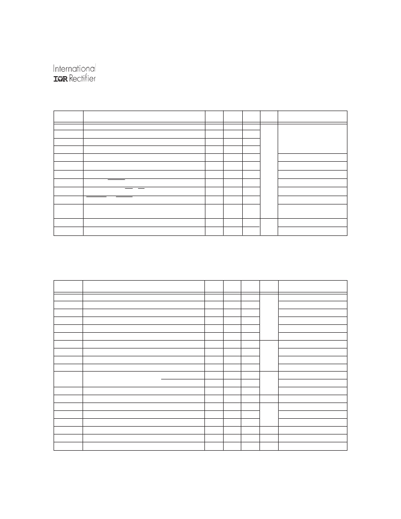
Static Electrical Characteristics
V
BIAS
(V
CC,
V
BS1,2,3
) = 15V unless otherwise specified and T
A
= 25
o
C. The V
IN,
V
TH
and I
IN
parameters are
referenced to V
SS
and are applicable to all six channels (H
S1,2,3
& L
S1,2,3
). The VO and IO parameters are
referenced to V
SS
and V
S1,2,3
and are applicable to the respective output leads: H
O1,2,3
or L
O1,2,3.
V
IH
V
IL
V
FCLR,IH
V
FCLR,IL
V
SD,TH+
V
SD,TH-
V
IT,TH+
V
IT,TH-
V
OH
V
OL
I
LK
Logic “0” Input Voltage (OUT = LO)
Logic “1” Input Voltage (OUT = HI)
Logic “0” Fault Clear Input Voltage
Logic “1” Fault Clear Input Voltage
SD Input Positive Going Threshold
SD Input Negative Going Threshold
I
ITRIP
Input Positive Going Threshold
I
ITRIP
Input Negative Going Threshold
High Level Output Voltage, VBIAS - VO
Low Level Output Voltage, VO
Offset Supply Leakage Current (IR2133/IR2135)
(IR2233/IR2235)
Quiescent VBS Supply Current
Quiescent VCC Supply Current
Logic “1” Input Bias Current (OUT = HI)
Logic “0” Input Bias Current (OUT = LO)
“High” Shutdown Bias Current
“Low” Shutdown Bias Current
“High” I
ITRIP
Bias Current
“Low” I
ITRIP
Bias Current
2.2
—
2.2
—
1.6
1.4
470
360
—
—
—
—
—
—
—
—
—
—
—
—
—
—
—
—
1.9
1.7
570
460
—
—
—
—
50
4
200
100
30
—
30
—
—
0.8
—
0.8
2.2
2.0
670
560
100
100
50
50
100
8
350
250
100
100
100
100
V
IN
= 0V, IO = 0A
V
IN
= 5V, IO = 0A
V
B1,2,3
=V
S1,2,3
= 600V
V
B1,2,3
=V
S1,2,3
= 1200V
V
IN
= 0V or 5V
V
IN
= 0V or 5V
V
IN
= 0V
V
IN
= 5V
SD = 5V
SD = 0V
I
ITRIP
= 5V
I
ITRIP
= 0V
I
QBS
I
QCC
I
IN+
I
IN-
I
SD+
I
SD-
I
ITRIP+
I
ITRIP-
mA
nA
μA
nA
Symbol
V
μA
Dynamic Electrical Characteristics
V
BIAS (
V
CC,
V
BS1,2,3)
= 15V,
V
S1,2,3
=
V
SS
,
T
A
= 25
o
C
and
C
L
= 1000
p
F
unless otherwise specified.
Definition
Turn-on propagation delay
Turn-off propagation delay
Turn-on rise time
Turn-off fall time
SD to output shutdown propagation delay
ITRIP to output shutdown propagation delay
ITRIP blanking time
ITRIP to FAULT propagation delay
Input filter time (HIN, LIN and SD)
FLT-CLR to FAULT clear time
Deadtime, LS turn-off to HS turn-on &
HS turn-off to LS turn-on
Amplifier slew rate (positive)
Amplifier slew rate (negative)
Min.
500
450
—
—
500
600
—
400
—
600
100
Typ.
750
700
90
40
750
850
400
650
310
850
250
Max. Units Test Conditions
1000
950
150
70
1000
1100
V
IN
,V
ITRIP
= 0 & 5V
—
ITRIP = 1V
900
V
IN
,V
ITRIP
= 0 & 5V
—
V
IN
= 0 & 5V
1100
V
IN
,V
ITRIP
= 0 & 5V
400
V
IN
= 0 & 5V
ton
toff
tr
tf
tsd
titrip
tbl
tflt
tfil,in
tfltclr
DT
V
IN
,V
SD
= 0 & 5V
SR+
SR-
5
2
10
2.5
—
—
Symbol
V/μs
ns
V
IN
= 0 & 5V
V
S1,2,3
= 0 to 600V
or 1200V
Definition Min. Typ. Max. Units Test Conditions
NOTE:
For high side PWM, HIN pulse width must be
≥ 1μ
sec
mV
μA
相關(guān)PDF資料 |
PDF描述 |
|---|---|
| IR2233J | 3-PHASE BRIDGE DRIVER |
| IR2233S | 3-PHASE BRIDGE DRIVER |
| IR2135J | 3-PHASE BRIDGE DRIVER |
| IR2135S | 3-PHASE BRIDGE DRIVER |
| IR2133 | 3-PHASE BRIDGE DRIVER |
相關(guān)代理商/技術(shù)參數(shù) |
參數(shù)描述 |
|---|---|
| IR2235SPbF | 功能描述:功率驅(qū)動(dòng)器IC 3 PHASE DRVR HI & LO SIDE INPUTS RoHS:否 制造商:Micrel 產(chǎn)品:MOSFET Gate Drivers 類型:Low Cost High or Low Side MOSFET Driver 上升時(shí)間: 下降時(shí)間: 電源電壓-最大:30 V 電源電壓-最小:2.75 V 電源電流: 最大功率耗散: 最大工作溫度:+ 85 C 安裝風(fēng)格:SMD/SMT 封裝 / 箱體:SOIC-8 封裝:Tube |
| IR2235STRPBF | 功能描述:功率驅(qū)動(dòng)器IC 3 PHASE DRVR HI & LO SIDE INPUTS RoHS:否 制造商:Micrel 產(chǎn)品:MOSFET Gate Drivers 類型:Low Cost High or Low Side MOSFET Driver 上升時(shí)間: 下降時(shí)間: 電源電壓-最大:30 V 電源電壓-最小:2.75 V 電源電流: 最大功率耗散: 最大工作溫度:+ 85 C 安裝風(fēng)格:SMD/SMT 封裝 / 箱體:SOIC-8 封裝:Tube |
| IR2237 | 制造商:IRF 制造商全稱:International Rectifier 功能描述:3-PHASE BRIDGE DRIVER |
| IR2237J | 制造商:IRF 制造商全稱:International Rectifier 功能描述:3-PHASE BRIDGE DRIVER |
| IR2237Q | 制造商:IRF 制造商全稱:International Rectifier 功能描述:3-PHASE BRIDGE DRIVER |
發(fā)布緊急采購(gòu),3分鐘左右您將得到回復(fù)。