- 您現(xiàn)在的位置:買賣IC網(wǎng) > PDF目錄377497 > IR21367J (International Rectifier) 3-PHASE BRIDGE DRIVER PDF資料下載
參數(shù)資料
| 型號(hào): | IR21367J |
| 廠商: | International Rectifier |
| 英文描述: | 3-PHASE BRIDGE DRIVER |
| 中文描述: | 3相橋式驅(qū)動(dòng)器 |
| 文件頁數(shù): | 4/36頁 |
| 文件大小: | 390K |
| 代理商: | IR21367J |
第1頁第2頁第3頁當(dāng)前第4頁第5頁第6頁第7頁第8頁第9頁第10頁第11頁第12頁第13頁第14頁第15頁第16頁第17頁第18頁第19頁第20頁第21頁第22頁第23頁第24頁第25頁第26頁第27頁第28頁第29頁第30頁第31頁第32頁第33頁第34頁第35頁第36頁
IR2136(2)(3)(5)(6)(7)(8)(J&S) & (PbF)
4
www.irf.com
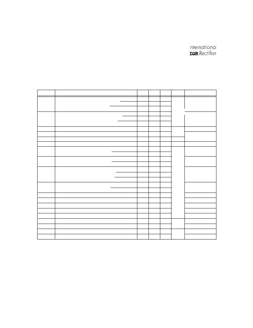
Static Electrical Characteristics cont.
V
BIAS
(V
CC
, V
BS
1,2,3) = 15V unless otherwise specified. The V
IN
, V
TH
and I
IN
parameters are referenced to V
SS
and
are applicable to all six channels (H
S
1,2,3 and L
S
1,2,3). The V
O
and I
O
parameters are referenced to COM and V
S
1,2,3
and are applicable to the respective output leads: H
O1,2,3
and L
O1,2,3.
Symbol
Definition
V
CCUV-
V
CC
and V
BS
supply undervoltage IR2136(8)
V
BSUV-
negative going threshold
IR21362
IR21363(5)(6)(7)
V
CCUVH
V
CC
and V
BS
supply undervoltage
IR2136
V
BSUVH
lockout hysteresis
IR21362
IR21363(5)
I
LK
Offset supply leakage current
I
QBS
Quiescent V
BS
supply current
I
QCC
Quiescent V
CC
supply current
V
IN, CLAMP
Input clamp voltage (HIN, LIN, ITRIP and EN)
I
LIN+
Input bias current (LOUT = HI) IR2136(2)(3)(5)
IR21366(7)(8)
I
LIN-
Input bias current (LOUT = LO) IR2136(2)(3)(5)
IR21366(7)(8)
I
HIN+
Input bias current (HOUT = HI)
IR2136(3)(5)
IR21362
IR21366(7)(8)
I
HIN-
Input bias current (HOUT = LO)
IR2136(3)(5)
IR21362(6)(7)(8)
I
ITRIP+
“high” ITRIP input bias current
I
ITRIP-
“l(fā)ow” ITRIP input bias current
I
EN+
“high” ENABLE input bias current
I
EN-
“l(fā)ow” ENABLE input bias current
I
RCIN
RCIN input bias current
I
O+
Output high short circuit pulsed current
I
O-
Output low short circuit pulsed current
R
ON,RCIN
RCIN low on resistance
R
ON,FLT
FAULT low on resistance
Min.
7.4
8.6
10.4
0.3
0.5
—
—
—
—
4.9
—
—
—
—
—
—
—
—
—
—
—
—
—
—
120
250
—
—
Typ. Max. Units Test Conditions
8.2
9.0
9.4
10.2
10.9
11.4
0.7
—
1.0
—
0.2
—
—
50
70
120
1.6
2.3
mA
5.2
5.5
V
200
300
0
1
100
220
0
1
200
300
30
100
0
1
100
220
0
1
30
100
0
1
30
100
0
1
0
1
200
—
350
—
50
100
50
100
V
B1,2,3
=V
S1,2,3
=600V
I
IN
=100
μ
A
V
LIN
= 5V
V
LIN
= 0V
V
HIN
= 5V
V
HIN
= 0V
V
ITRIP
= 5V
V
ITRIP
= 0V
V
ENABLE
= 5V
V
ENABLE
= 0V
V
RCIN
= 0V or 15V
V
O
=0V, PW
≤
10
μ
s
V
O
=15V, PW
≤
10
μ
s
V
IN
= 0V or 5V
μ
A
μ
A
mA
V
相關(guān)PDF資料 |
PDF描述 |
|---|---|
| IR21367S | 3-PHASE BRIDGE DRIVER |
| IR21367SPBF | 3-PHASE BRIDGE DRIVER |
| IR21368J | 3-PHASE BRIDGE DRIVER |
| IR21368PBF | 3-PHASE BRIDGE DRIVER |
| IR21368S | 3-PHASE BRIDGE DRIVER |
相關(guān)代理商/技術(shù)參數(shù) |
參數(shù)描述 |
|---|---|
| IR21367JPBF | 制造商:International Rectifier 功能描述:MOSFET DRIVER 3PH HIGH/LOW 21367 |
| IR21367PBF | 制造商:International Rectifier 功能描述:DRIVER MOSFET 3PH HIGH/LOW 21367 |
| IR21367S | 制造商:IRF 制造商全稱:International Rectifier 功能描述:3-PHASE BRIDGE DRIVER |
| IR21367SPBF | 制造商:International Rectifier 功能描述:DRIVER MOSFET 3PH HIGH/LOW 21367 |
| IR21368 | 制造商:IRF 制造商全稱:International Rectifier 功能描述:3-PHASE BRIDGE DRIVER |
發(fā)布緊急采購,3分鐘左右您將得到回復(fù)。