- 您現(xiàn)在的位置:買賣IC網(wǎng) > PDF目錄360899 > IP1R1715-T (TT electronics Semelab Limited) CANMS3126F16-8PXF0 PDF資料下載
參數(shù)資料
| 型號: | IP1R1715-T |
| 廠商: | TT electronics Semelab Limited |
| 英文描述: | CANMS3126F16-8PXF0 |
| 中文描述: | 3安培固定負(fù)電壓調(diào)節(jié)器 |
| 文件頁數(shù): | 4/4頁 |
| 文件大小: | 32K |
| 代理商: | IP1R1715-T |
LAB
SEME
IP1R17A
IP3R17A
IP1R17
A
IP3R17
A
Semelab plc.
Telephone (01455) 556565. Telex: 341927. Fax (01455) 552612.
Prelim. 4/96
IP1R17A–15
IP3R17A–15
Min.
Typ.
-15.15
IP1R17–15
IP3R17–15
Min.
Typ.
-15.45
Parameter
Test Conditions
2
Max.
-14.85
Max.
-14.55
Units
V
V
O
V
O
V
I
V
O
I
O
I
Q
I
Q
V
D
I
PEAK
I
SC
e
n
R
θ
JC
Output Voltage
Line Regulation
Load Regulation
Quiescent Current
Quiescent Current
Change
Dropout Voltage
Ripple Rejection
Thermal Regulation
Peak Output Current
Short Circuit Current
Output Noise Voltage
Thermal Resistance
Junction to Case
I
O
= -5mA to -3A
P
OUT
≤
P
MAX
T
J
= Over Temp. Range
1
V
IN
= -17.5V to -35V
I
O
= -5mA
3
I
O
= -5mA to -3A
3
V
IN
= -18V to -30V
T
J
= Over Temp. Range
1
T
J
= Over Temp. Range
1
T
J
= Over Temp. Range
1
I
O
= -5mA
I
O
= -5mA to -3A
T
J
= Over Temp. Range
1
I
O
= -5mA
T
J
= Over Temp. Range
1
I
O
= -3A
T
J
= Over Temp. Range
1
I
O
= -1A
T
J
= Over Temp. Range
1
t
p
= 20ms
V
IN
= -20V
V
IN
= -20V
V
IN
= -35V
f = 10Hz to 100kHz
V
IN
= -17.5V to -35V
V
OUT
= 300mV
f = 120Hz
P = P
MAX
T
J
= Over Temp. Range
1
K Package
G, T Package
-15
-15.75
-14.25
16
80
32
160
32
160
64
320
5
10
5
2.2
3
50
70
0.002
0.02
-6.5
-4.5
-2.3
-1
90
1.5
2.5
3
4
-15
-15.45
-14.55
8
40
16
80
16
80
32
160
5
10
5
2.2
3
50
70
0.002
0.01
-6.5
-4.5
-2.3
-1
90
1.5
2.5
3
4
V
mV
mV
mA
mA
V
dB
%/W
A
A
μ
V
°C/W
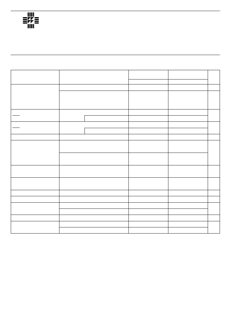
ELECTRICAL CHARACTERISTICS
(T
J
= 25°C unless otherwise stated)
Notes
1) Applies over full temperature range:–
T
J
= –55 to +150°C for IP1R17A–15 / IP1R17–15
T
J
=
0 to +125°C for IP3R17A–15 / IP3R17–15
All other specifications apply at T
C
= 25°C unless otherwise stated.
2) Test conditions unless otherwise stated:–
V
IN
= -20V , I
OUT
= -1.5A .
Although Power Dissipation is internally limited, these specifications apply for Power Dissipation up to 30W for the TO–3
Package, and 20W for the TO–220 and TO–257 Packages.
3) Load and Line regulation are electrically independent and are measured using pulse techniques at low duty cycle in order to
maintain constant junction temperature. To determine the effects on the output voltage due to device heating, refer to thermal
regulation specification.
相關(guān)PDF資料 |
PDF描述 |
|---|---|
| IP1R17A | 3 AMP FIXED NEGATIVE VOLTAGE REGULATORS |
| IP3R17A-05 | CAT5E PATCH CORD, 50FT PURPLE, MOLDED |
| IP1R17A-05 | CAT5E PATCH CORD, 100FT PURPLE, MOLDED |
| IP3R17A-12 | CAT5E PATCH CORD, 25FT ORANGE, MOLDED |
| IP1R17A-12 | CAT5E PATCH CORD, 30FT ORANGE, MOLDED |
相關(guān)代理商/技術(shù)參數(shù) |
參數(shù)描述 |
|---|---|
| IP1R17A | 制造商:SEME-LAB 制造商全稱:Seme LAB 功能描述:3 AMP FIXED NEGATIVE VOLTAGE REGULATORS |
| IP1R17A_07 | 制造商:SEME-LAB 制造商全稱:Seme LAB 功能描述:1 AMP POSITIVE VOLTAGE REGULATOR |
| IP1R17A-05 | 制造商:SEME-LAB 制造商全稱:Seme LAB 功能描述:3 AMP FIXED NEGATIVE VOLTAGE REGULATORS |
| IP1R17A05-G | 制造商:SEME-LAB 制造商全稱:Seme LAB 功能描述:3 AMP FIXED NEGATIVE VOLTAGE REGULATORS |
| IP1R17A05-K | 制造商:SEME-LAB 制造商全稱:Seme LAB 功能描述:3 AMP FIXED NEGATIVE VOLTAGE REGULATORS |
發(fā)布緊急采購,3分鐘左右您將得到回復(fù)。