- 您現(xiàn)在的位置:買賣IC網 > PDF目錄360862 > INA117SM High Common-Mode Voltage DIFFERENCE AMPLIFIER PDF資料下載
參數(shù)資料
| 型號: | INA117SM |
| 元件分類: | 差分放大器 |
| 英文描述: | High Common-Mode Voltage DIFFERENCE AMPLIFIER |
| 中文描述: | 高共模電壓差分放大器 |
| 文件頁數(shù): | 9/14頁 |
| 文件大小: | 192K |
| 代理商: | INA117SM |
9
INA117
In all cases, the sense resistor imbalances the input resistor
matching of the INA117, degrading its CMR. Also, the input
impedance of the INA117 loads R
S
, causing gain error in the
voltage-to-current conversion. Both of these errors can be
easily corrected.
The CMR error can be corrected with the addition of a
compensation resistor, R
C
, equal in value to R
S
as shown in
Figures 4, 5, and 6. If R
S
is less than 20
, the degradation
in CMR is negligible and R
C
can be omitted. If R
S
is larger
than approximately 2k
, trimming R
C
may be required to
achieve greater than 86dB CMR. This is because the actual
INA117 input impedances have 1% typical mismatch.
If R
S
is more than approximately 100
, the gain error will
be greater than the 0.02% specification of the INA117. This
gain error can be corrected by slightly increasing the value
of R
S
. The corrected value, R
S
', can be calculated by—
R
380k
380k
– R
S
R
S
' = ——————
Example: For a 1V/mA transfer function, the nominal,
uncorrected value for R
S
would be 1k
. A slightly larger
value, R
S
' = 1002.6
, compensates for the gain error due to
loading.
The 380k
term in the equation for R
S
' has a tolerance of
±
25%, so sense resistors above approximately 400
may
require trimming to achieve gain accuracy better than 0.02%.
Of course, if a buffer amplifier is added as shown in Figure
7, both inputs see a low source impedance, and the sense
resistor is not loaded. As a result, there is no gain error or
CMR degradation. The buffer amplifier can operate as a
unity gain buffer or as an amplifier with non-inverting gain.
Gain added ahead of the INA117 improves both CMR and
signal-to-noise. Added gain also allows a lower voltage drop
across the sense resistor. The OPA1013 is a good choice for
the buffer amplifier since both its input and output can swing
close to its negative power supply.
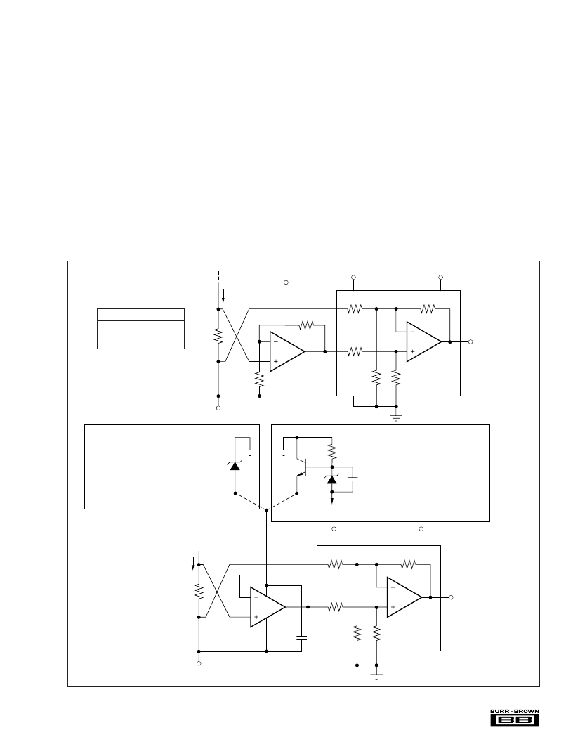
FIGURE 7. Current Sensing with Input Buffer.
V
X
V
1
–21V to +10V
–5V to –36V
–20V to –51V
+15V
Ground
–15V
380k
380k
380k
21.1k
20k
4
7
2
3
8
1
5
V
O
= I R
S
(1 +R
6
I
–15V
+15V
2
R
1
R
2
*
1/2
OPA1013
V
1
R *
1
R
S
–V
X
380k
380k
380k
21.1k
20k
4
7
2
3
8
1
5
V
O
= I R
S
6
I
V–
V+
1/2
OPA1013
R
S
0.1μF
IN4702
MPS-A42
180k
0.01μF
V
Z
or
–V
X
–V
X
Op amp power can be derived with voltage-
dropping zener diode if –V
X
power is relatively
constant.
|V
| = (5V to 36V) + V
Z
e.g., If V
Z
is 50V then V
X
= –55V to –86V.
Regulated power for op amp allows –V
X
power to vary over wide range.
V
X
= –30V to –200V
*Or connect as buffer (R
2
= 0, omit R
1
).
相關PDF資料 |
PDF描述 |
|---|---|
| INA118UB | CAT6 SOL PC PVC WHI 2FT PVC SOLID PATCH CORD |
| INA118 | Precision, Low Power INSTRUMENTATION AMPLIFIER |
| INA118P | Precision, Low Power INSTRUMENTATION AMPLIFIER |
| INA118PB | RES,THKF,68.0,1.0%,100PPM,0.125W |
| INA118U | Precision, Low Power INSTRUMENTATION AMPLIFIER |
相關代理商/技術參數(shù) |
參數(shù)描述 |
|---|---|
| INA117SM | 制造商:Texas Instruments 功能描述:IC DIFF AMP 200KHZ 2.6V/ |
| INA117SMQ | 功能描述:差分放大器 High Common-Mode Voltage RoHS:否 制造商:Texas Instruments 通道數(shù)量:1 Channel 帶寬:2.4 GHz 可用增益調整:6 dB to 26 dB 輸入補償電壓: 共模抑制比(最小值):- 40 dB 工作電源電壓:4.75 V to 5.25 V 電源電流:100 mA 最大工作溫度:+ 85 C 最小工作溫度:- 40 C 安裝風格:SMD/SMT 封裝 / 箱體:WQFN-24 封裝:Reel |
| INA118 | 制造商:BB 制造商全稱:BB 功能描述:Precision, Low Power INSTRUMENTATION AMPLIFIER |
| INA118P | 功能描述:儀表放大器 Precision Low Power Instrumentation Amp RoHS:否 制造商:Texas Instruments 通道數(shù)量: 輸入補償電壓:150 V 可用增益調整: 最大輸入電阻:10 kOhms 共模抑制比(最小值):88 dB 工作電源電壓:2.7 V to 36 V 電源電流:200 uA 最大工作溫度:+ 125 C 最小工作溫度:- 40 C 封裝 / 箱體:MSOP-8 封裝:Bulk |
| INA118P | 制造商:Texas Instruments 功能描述:IC AMP INSTRUMENTATION DIP8 118 |
發(fā)布緊急采購,3分鐘左右您將得到回復。