- 您現(xiàn)在的位置:買賣IC網(wǎng) > PDF目錄360862 > INA117P High Common-Mode Voltage DIFFERENCE AMPLIFIER PDF資料下載
參數(shù)資料
| 型號(hào): | INA117P |
| 元件分類: | 差分放大器 |
| 英文描述: | High Common-Mode Voltage DIFFERENCE AMPLIFIER |
| 中文描述: | 高共模電壓差分放大器 |
| 文件頁數(shù): | 6/14頁 |
| 文件大?。?/td> | 192K |
| 代理商: | INA117P |
6
INA117
APPLICATION INFORMATION
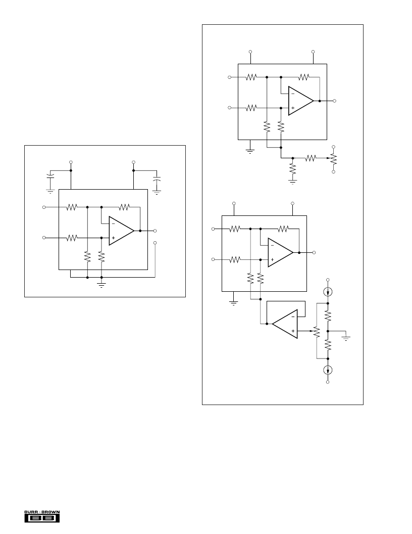
Figure 1 shows the basic connections required for operation.
Applications with noisy or high impedance power supply lines
may require decoupling capacitors close to the device pins.
The output voltage is equal to the differential input volt-
age between pins 2 and 3. The common mode input
voltage is rejected.
Internal circuitry connected to the compensation pin 8 can-
cels the parasitic distributed capacitance between the feed-
back resistor, R
2
, and the IC substrate. For specified dy-
namic performance, pin 8 should be grounded or connected
through a 0.1
μ
F capacitor to an AC ground such as V+.
COMMON-MODE REJECTION
Common-mode rejection (CMR) of the INA117 is depend-
ent on the input resistor network, which is laser-trimmed for
accurate ratio matching. To maintain high CMR, it is impor-
tant to have low source impedances driving the two inputs.
A 75
resistance in series with pin 2 or 3 will decrease CMR
from 86dB to 72dB.
Resistance in series with the reference pins will also degrade
CMR. A 4
resistance in series with pin 1 or 5 will decrease
CMRR from 86dB to 72dB.
Most applications do not require trimming. Figures 2 and 3
show optional circuits that may be used for trimming offset
voltage and common-mode rejection.
TRANSFER FUNCTION
Most applications use the INA117 as a simple unity-gain
difference amplifier. The transfer function is:
V
O
= V
3
– V
2
V
3
and V
2
are the voltages at pins 3 and 2.
FIGURE 1. Basic Power and Signal Connections.
+
+
380k
380k
380k
21.1k
20k
4
7
2
3
8
1
5
–15V
+15V
1μF
Tantalum
1μF
Tantalum
–In = V
2
+In = V
3
V
O
= V
3
– V
2
6
R
1
R
2
R
4
R
5
R
3
380k
380k
380k
21.1k
20k
4
7
2
3
8
1
5
V–
V+
V
2
V
3
V
O
= V
3
– V
2
6
100k
10
50k
±1.5mV
Range
–15V
+15V
380k
380k
380k
21.1k
20k
4
7
2
3
8
1
5
V–
V+
V
2
V
3
V = V – V
6
10k
±10mV
100
100
V+
V–
100μA
1/2 REF200
100μA
1/2 REF200
OPA27
Offset adjustment is regulated—
insensitive to power supply variations.
(a)
(b)
FIGURE 2. Offset Voltage Trim Circuits.
Some applications, however, apply voltages to the reference
terminals (pins 1 and 5). A more complete transfer function
is:
V
O
= V
3
– V
2
+ 19 V
5
– 18 V
1
V
5
and V
1
are the voltages at pins 5 and 1.
相關(guān)PDF資料 |
PDF描述 |
|---|---|
| INA117SM | High Common-Mode Voltage DIFFERENCE AMPLIFIER |
| INA118UB | CAT6 SOL PC PVC WHI 2FT PVC SOLID PATCH CORD |
| INA118 | Precision, Low Power INSTRUMENTATION AMPLIFIER |
| INA118P | Precision, Low Power INSTRUMENTATION AMPLIFIER |
| INA118PB | RES,THKF,68.0,1.0%,100PPM,0.125W |
相關(guān)代理商/技術(shù)參數(shù) |
參數(shù)描述 |
|---|---|
| INA117P | 制造商:BURR-BROWN 功能描述:IC AMP DIFF UNITY GAIN DIP8 117 制造商:Texas Instruments 功能描述:INST AMP HI SPEED 200KHZ DIP8 |
| INA117P-BI | 功能描述:差分放大器 V Diff Amp RoHS:否 制造商:Texas Instruments 通道數(shù)量:1 Channel 帶寬:2.4 GHz 可用增益調(diào)整:6 dB to 26 dB 輸入補(bǔ)償電壓: 共模抑制比(最小值):- 40 dB 工作電源電壓:4.75 V to 5.25 V 電源電流:100 mA 最大工作溫度:+ 85 C 最小工作溫度:- 40 C 安裝風(fēng)格:SMD/SMT 封裝 / 箱體:WQFN-24 封裝:Reel |
| INA117PG4 | 功能描述:差分放大器 V Diff Amp RoHS:否 制造商:Texas Instruments 通道數(shù)量:1 Channel 帶寬:2.4 GHz 可用增益調(diào)整:6 dB to 26 dB 輸入補(bǔ)償電壓: 共模抑制比(最小值):- 40 dB 工作電源電壓:4.75 V to 5.25 V 電源電流:100 mA 最大工作溫度:+ 85 C 最小工作溫度:- 40 C 安裝風(fēng)格:SMD/SMT 封裝 / 箱體:WQFN-24 封裝:Reel |
| INA117SM | 功能描述:差分放大器 High Common-Mode Voltage RoHS:否 制造商:Texas Instruments 通道數(shù)量:1 Channel 帶寬:2.4 GHz 可用增益調(diào)整:6 dB to 26 dB 輸入補(bǔ)償電壓: 共模抑制比(最小值):- 40 dB 工作電源電壓:4.75 V to 5.25 V 電源電流:100 mA 最大工作溫度:+ 85 C 最小工作溫度:- 40 C 安裝風(fēng)格:SMD/SMT 封裝 / 箱體:WQFN-24 封裝:Reel |
| INA117SM | 制造商:Texas Instruments 功能描述:IC DIFF AMP 200KHZ 2.6V/ |
發(fā)布緊急采購,3分鐘左右您將得到回復(fù)。