- 您現(xiàn)在的位置:買賣IC網(wǎng) > PDF目錄360862 > INA116P Very High Accuracy Instrumentation Amplifier PDF資料下載
參數(shù)資料
| 型號(hào): | INA116P |
| 元件分類: | 測(cè)量放大器 |
| 英文描述: | Very High Accuracy Instrumentation Amplifier |
| 中文描述: | 極高精度儀表放大器 |
| 文件頁(yè)數(shù): | 8/9頁(yè) |
| 文件大小: | 246K |
| 代理商: | INA116P |
INA116
8
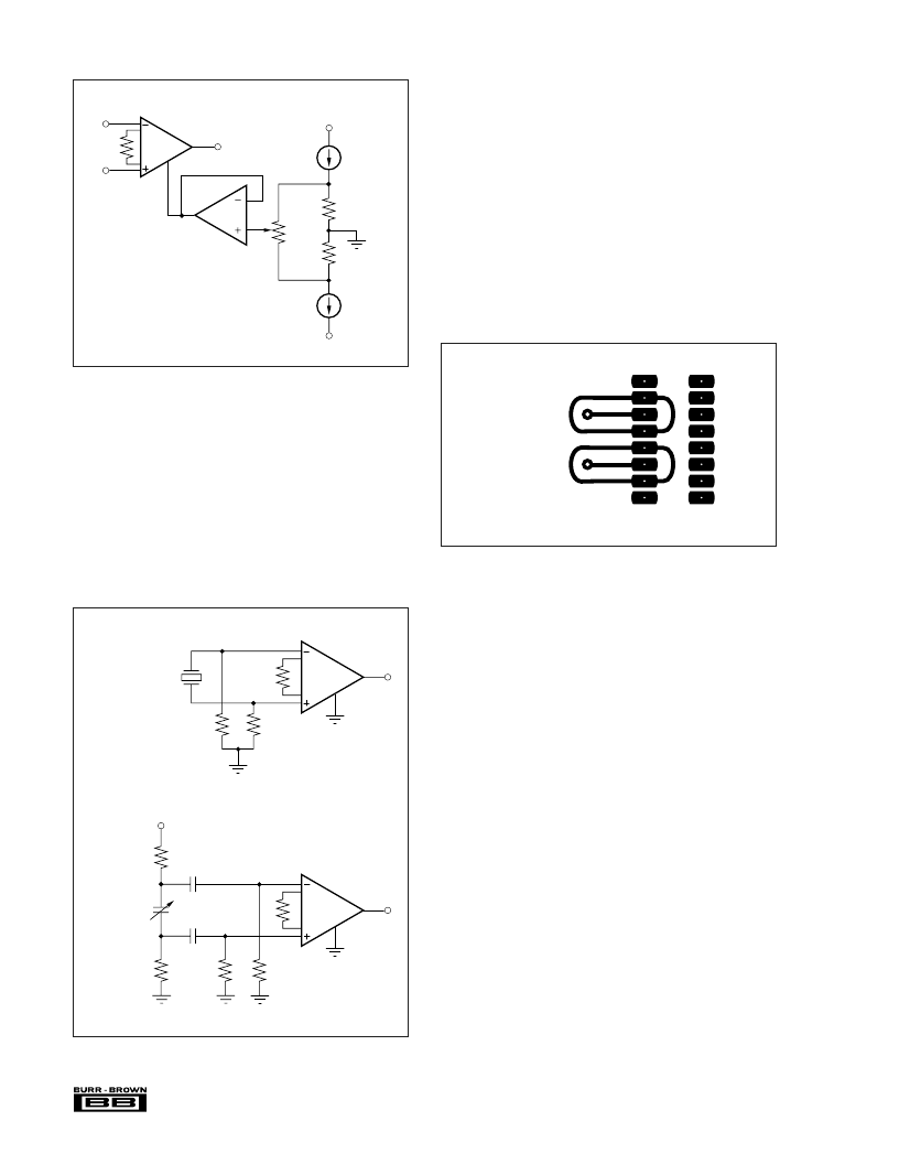
FIGURE 2. Optional Trimming of Output Offset Voltage.
INPUT BIAS CURRENT RETURN PATH
Input circuitry must provide an input bias current path for
proper operation. Figure 3 shows resistors R
1
and R
2
to
provide an input current path. Without these resistors, the
inputs would eventually float to a potential that exceeds the
common-mode range of the INA116 and the input amplifiers
would saturate. Because of its exceedingly low input bias
current, improperly biased inputs may operate normally for
a period of time after power is first applied, or operate
intermittently.
CIRCUIT BOARD LAYOUT AND ASSEMBLY
Careful circuit board layout and assembly techniques are
required to achieve the exceptionally low input bias current
performance of the INA116. Guard terminals adjacent to
both inputs make it easy to properly guard the critical input
terminal layout. Since traces are not required to run between
device pins, this layout is easily accomplished, even with the
surface mount package. The guards should completely en-
circle their respective input connections—see Figure 4. Both
sides of the circuit board should be guarded, even if only one
side has an input terminal conductor. Route any time-
varying signals away from the input terminals. Solder mask
should not cover the input and guard traces since this can
increase leakage.
FIGURE 3. Providing An Input Bias Current Path.
FIGURE 4. Circuit Board Guard Layout.
After assembly, the circuit board should be cleaned. Com-
mercial solvents should be chosen according to the soldering
method and flux used. Solvents should be cleaned and
replaced often. Solvent cleaning should be followed by a de-
ionized water rinse and 85
°
C bake out.
Sockets can be used, but select and evaluate them carefully
for best results. Use caution when installing the INA116 in
a socket. Careless handling can contaminate the plastic near
the input pins, dramatically increasing leakage current.
A proven low leakage current assembly method is to bend
the input pins outward so they do not contact the circuit
board. Input connections are made in air and soldered
directly to the input pin. This technique is often not practical
or production-worthy. It is, however, a useful technique for
evaluation and testing and provides a benchmark with which
to compare other wiring techniques. The circuit board guard-
ing techniques discussed normally reduce leakage to accept-
able levels.
A solid mechanical assembly is required for good results.
Nearby plastic parts can be especially troublesome since a
static charge can develop and the slightest motion or vibra-
tion will couple charge to the inputs. Place a Faraday shield
around the whole amplifier and input connection assembly
to eliminate stray fields.
INA116
100M
R
1
100M
R
2
V
O
V
O
INA116
100M
R
2
100M
R
1
100M
100M
Polarizing
Voltage
Capacitive
Sensor
Crystal or
Ceramic
Transducer
Guard Top and
Bottom of Circuit Board.
INA116
V
IN
V
IN
R
G
–
+
10k
(1)
V
O
OPA131
Ref
±10mV
Adjustment Range
100
(1)
100
(1)
100μA
1/2 REF200
100μA
1/2 REF200
V+
V–
NOTE: (1) For wider trim range required
in high gains, scale resistor values larger
相關(guān)PDF資料 |
PDF描述 |
|---|---|
| INA116U | Very High Accuracy Instrumentation Amplifier |
| INA117KU | High Common-Mode Voltage DIFFERENCE AMPLIFIER |
| INA117AM | High Common-Mode Voltage DIFFERENCE AMPLIFIER |
| INA117BM | High Common-Mode Voltage DIFFERENCE AMPLIFIER |
| INA117 | High Common-Mode Voltage DIFFERENCE AMPLIFIER |
相關(guān)代理商/技術(shù)參數(shù) |
參數(shù)描述 |
|---|---|
| INA116PA | 功能描述:儀表放大器 Ultra Low Input Bias Current RoHS:否 制造商:Texas Instruments 通道數(shù)量: 輸入補(bǔ)償電壓:150 V 可用增益調(diào)整: 最大輸入電阻:10 kOhms 共模抑制比(最小值):88 dB 工作電源電壓:2.7 V to 36 V 電源電流:200 uA 最大工作溫度:+ 125 C 最小工作溫度:- 40 C 封裝 / 箱體:MSOP-8 封裝:Bulk |
| INA116PA | 制造商:Texas Instruments 功能描述:IC AMP INSTRUMENTATION DIP16 116 |
| INA116PAG4 | 功能描述:儀表放大器 Ultra Low Input Bias Current RoHS:否 制造商:Texas Instruments 通道數(shù)量: 輸入補(bǔ)償電壓:150 V 可用增益調(diào)整: 最大輸入電阻:10 kOhms 共模抑制比(最小值):88 dB 工作電源電壓:2.7 V to 36 V 電源電流:200 uA 最大工作溫度:+ 125 C 最小工作溫度:- 40 C 封裝 / 箱體:MSOP-8 封裝:Bulk |
| INA116U | 制造商:BB 制造商全稱:BB 功能描述:Ultra Low Input Bias Current INSTRUMENTATION AMPLIFIER |
| INA116UA | 功能描述:儀表放大器 Ultra Low Input Bias Current RoHS:否 制造商:Texas Instruments 通道數(shù)量: 輸入補(bǔ)償電壓:150 V 可用增益調(diào)整: 最大輸入電阻:10 kOhms 共模抑制比(最小值):88 dB 工作電源電壓:2.7 V to 36 V 電源電流:200 uA 最大工作溫度:+ 125 C 最小工作溫度:- 40 C 封裝 / 箱體:MSOP-8 封裝:Bulk |
發(fā)布緊急采購(gòu),3分鐘左右您將得到回復(fù)。