- 您現(xiàn)在的位置:買賣IC網(wǎng) > PDF目錄67720 > IMISM532AXB (CYPRESS SEMICONDUCTOR CORP) OTHER CLOCK GENERATOR, PDSO16 PDF資料下載
參數(shù)資料
| 型號(hào): | IMISM532AXB |
| 廠商: | CYPRESS SEMICONDUCTOR CORP |
| 元件分類: | 時(shí)鐘產(chǎn)生/分配 |
| 英文描述: | OTHER CLOCK GENERATOR, PDSO16 |
| 封裝: | SOIC-16 |
| 文件頁(yè)數(shù): | 4/14頁(yè) |
| 文件大小: | 132K |
| 代理商: | IMISM532AXB |
第1頁(yè)第2頁(yè)第3頁(yè)當(dāng)前第4頁(yè)第5頁(yè)第6頁(yè)第7頁(yè)第8頁(yè)第9頁(yè)第10頁(yè)第11頁(yè)第12頁(yè)第13頁(yè)第14頁(yè)
+/+
YJGP VKOKPI KU ETKVKECN
SM532
Approved Product
Low EMI Sprectum Spread Clock
International Microcircuits,Inc.
8/31/98
525 Los Coches St., Milpitas, 95035 408-263-6300, FAX 408-263-6571
Rev. 1.4
http:/www.imicorp.com
Page 12 of 14
As can be seen from the figure above, the Fout/Time profile progresses through frequencies depending on where
it is in the sweep. If the frequency is in the middle of the sweep, the rate of change is slower compared to the rate
at the extremes of the band. When the frequency is nearing the end of the band, it is moving through these
frequencies faster, since it has to sweep through these same frequencies again after reversing direction. This
modulation profile is one of the key elements to the SM532. Using a linear sweep through all frequencies would
not give as good of results in EMI reduction.
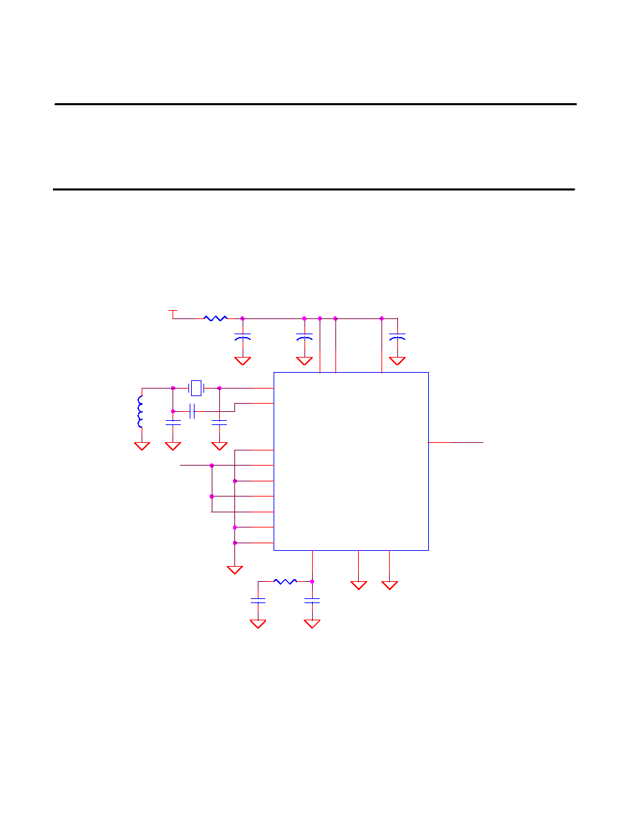
APPLICATION NOTES AND SCHEMATICS
The schematic figure shown below is a simple minimum component application example of an SM532 design. In
the case shown below, the control lines are configured for the following parameters;
Input Frequency: Mid-Range
Multiplier: X1
Modulation: 2.50%
SSON: On
Refer to loop filter values on Table 8, for operation at 3.3 Volts DC.
* L1 and C4 are required when Y1 is a 3rd. overtone crystal.
Figure 9. Application Schematic
The SM532 has an internal Analog Power and Ground and a Digital Power and Ground. In the example above,
the digital and analog circuits are connected together. If noise is a concern, it is recommended that the Analog
and Digital Power and Grounds be separated. The loop filter shown above is recommended for operation at 3.14 -
3.47 VDC. This filter can also be used in 5.0 VDC operations when operating in the low frequency end of each of
the three input frequency ranges. Refer to table 8 on page 6 for complete information. Also note, the crystal, Y1,
is a third overtone 50 Mhz crystal, which requires an inductor and decoupling capacitor to OSCout.
VCC = 3.3 VDC
Modulated Clock
Output
*
VDD
C5
27 pf.
Y1
50 MHz
C8
27 pf.
C1
22 uf.
C2
0.1 uf.
R2
10 ohm.
C3
0.1 uf.
C7
1000 pf.
C6
10,000 pf.
R1
1 K
L1
330 nh.
SM532
OSCin
1
OSCout
2
DVDD
16
DVSS
15
AVSS
6
AVDD
3
Fout
12
R0
14
R1
13
S0
4
S1
7
S2
11
S3
9
LF
5
SSON
8
DVDD
10
C4
.033 uf.
相關(guān)PDF資料 |
PDF描述 |
|---|---|
| IMSA113-J20S | ACTIVE DELAY LINE, PQCC44 |
| IMSB419-4 | SPECIALTY MICROPROCESSOR CIRCUIT, XMA16 |
| IMSC011-E20S | 1 CHANNEL(S), 20M bps, SERIAL COMM CONTROLLER, PDSO28 |
| IMSC011-P20S | 1 CHANNEL(S), 20M bps, SERIAL COMM CONTROLLER, PDIP28 |
| IMSC011-W20S | 1 CHANNEL(S), 20M bps, SERIAL COMM CONTROLLER, CQCC28 |
相關(guān)代理商/技術(shù)參數(shù) |
參數(shù)描述 |
|---|---|
| IMISM532AXBT | 制造商:Cypress Semiconductor 功能描述: |
| IMISM560BSZ | 制造商:Rochester Electronics LLC 功能描述:- Bulk |
| IMISM560BZ | 制造商:Cypress Semiconductor 功能描述:PLL Frequency Synthesizer Single 25MHz to 108MHz 8-Pin SOIC 制造商:Rochester Electronics LLC 功能描述:TIMING DEVICE - Bulk |
| IMISM560BZT | 制造商:Cypress Semiconductor 功能描述:PLL Frequency Synthesizer Single 25MHz to 108MHz 8-Pin SOIC T/R |
| IMISM561 | 制造商:CYPRESS 制造商全稱:Cypress Semiconductor 功能描述:Spread Spectrum Clock Generator |
發(fā)布緊急采購(gòu),3分鐘左右您將得到回復(fù)。