- 您現(xiàn)在的位置:買賣IC網(wǎng) > PDF目錄67720 > IMISG522BX (CYPRESS SEMICONDUCTOR CORP) 120 MHz, OTHER CLOCK GENERATOR, PDSO16 PDF資料下載
參數(shù)資料
| 型號: | IMISG522BX |
| 廠商: | CYPRESS SEMICONDUCTOR CORP |
| 元件分類: | 時鐘產(chǎn)生/分配 |
| 英文描述: | 120 MHz, OTHER CLOCK GENERATOR, PDSO16 |
| 封裝: | 0.300 INCH, PLASTIC, SOIC-16 |
| 文件頁數(shù): | 7/12頁 |
| 文件大?。?/td> | 122K |
| 代理商: | IMISG522BX |
SG521/22/24/28
Spread Spectrum Clock Generator
Approved Product
INTERNATIONAL MICROCIRCUITS,INC. 525 LOS COCHES ST.,
Rev. 2.0
5/25/2000
MILPITAS, CA 95035 408-263-6300, FAX 408-263-6571
Page 4 of 12
http:/www.imicorp.com
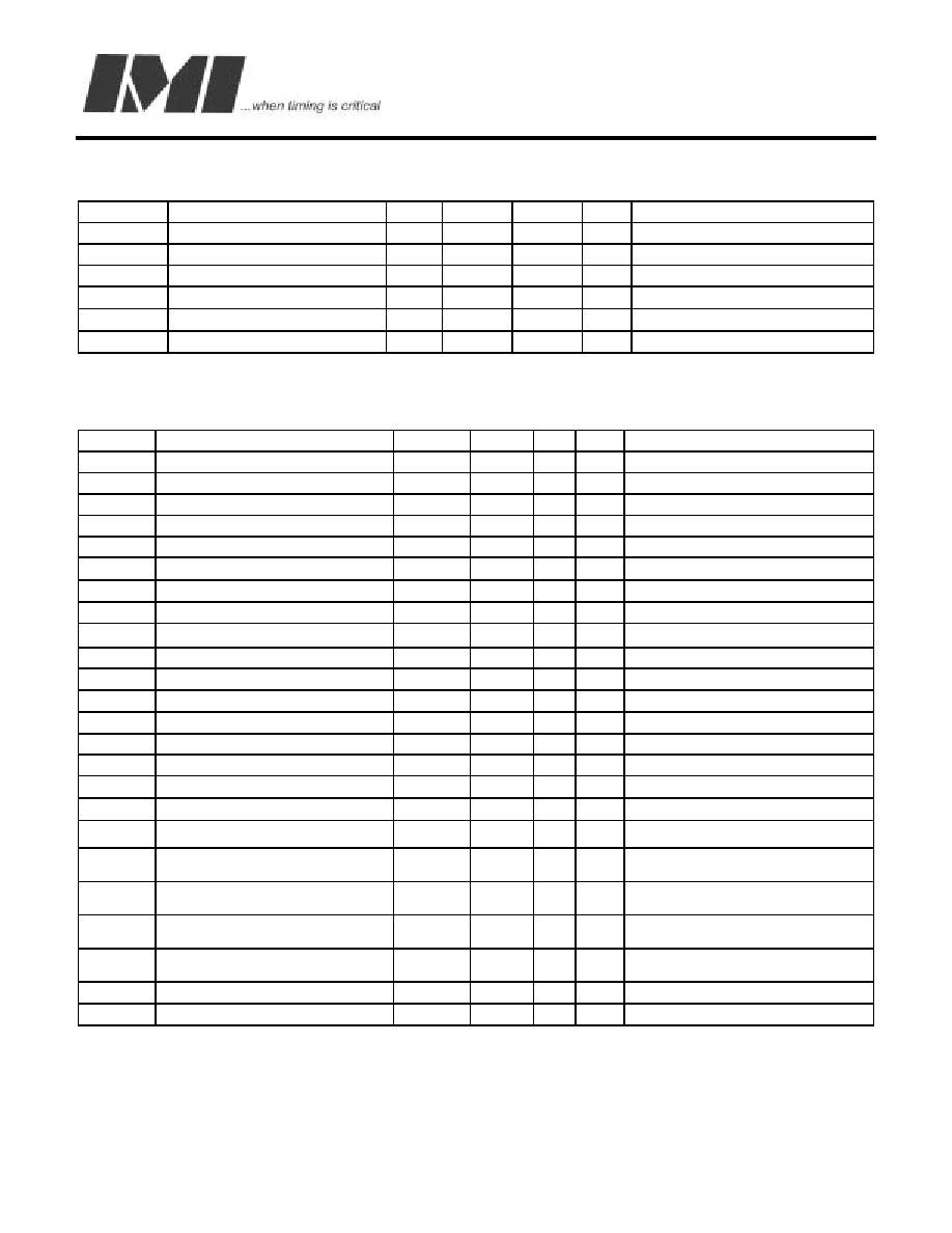
Absolute Maximum Ratings
Symbol
Parameter
Min.
Typical
Max.
Unit
Conditions
VDD
Supply Voltage
3.135
3.3/5.0
7.0
V
Measured from pin 1, 6 or 15 to VSS
Vimax
Input Voltage Relative to VSS
-0.3
-
VDD+0.3
V
Pins 5, 7, 8, 9, 10, 12, 14 and 16.
Vomax
Output Voltage Relative to VSS
-0.3
-
VDD+0.3
V
Pins 12 and 14
Top
Operating Temperature
0
-
70
°C
Refer to QA report.
Tst
Storage Temperature
-55
-
150
°C
Refer to QA report.
Tjc
Soldering Junction Temperature
-
300
°C
10 seconds soldering
Note: Operation at any Absolute Maximum Rating is not implied. Refer to DC Electrical Characteristics for proper Operating Range.
Test Conditions: VDD=3.3/5.0 V (+/-10%), CL=15pF, Operating Temperature = 0 to 70
°C unless otherwise specified
DC Electrical Characteristics
Symbol
Parameter
Min.
Typical Max.
Unit
Conditions
VDD
Power Supply Voltage, Operating
3.135
3.3/5.0
5.5
V
Measured from pin 1, 6 or 15 to VSS
OSCin-cl
Oscillator Input Load Capacitance
3
pF
Pin 2.
OSCout-cl Oscillator Output Load Capacitance
5
pF
Pin 3.
Vinl
Input Voltage, Low
-
0.8
V
Pins 5, 7, 8, 9, 10, 12, 14 and 16.
Vinh
Input Voltage, High
2.0
-
V
Pins 5, 7, 8, 9, 10, 12, 14 and 16.
Iinl
Input Current, Low
-
50
A
Pins 5, 7, 8, 9, 10, 12, 14 and 16.
Iinh
Input Current, High
-
50
A
Pins 5, 7, 8, 9, 10, 12, 14 and 16.
VOL1
Output Low Voltage
-
0.4
Vdc
IL = 12mA, VDD = 5V
VOH1
Output High Voltage
VDD-1.0
-
Vdc
IL = 12mA, VDD = 5V
VOL2
Output Low Voltage
-
0.4
Vdc
IL = 10mA, VDD = 3.3V
VOH2
Output High Voltage
VDD-0.8
-
Vdc
IL = 10mA, VDD = 3.3V
Rpu/Rpd
Pull-up/down Resistors
100
150
250
K
Pins 5, 7, 8, 9, 10, 12, 14 and 16.
Zo
Clock Output Impedance, PRCLK
-
12.5
-
Ohms
VDD = 5.00 VDC
Zo
Clock Output Impedance, MPCLK
-
23.0
-
Ohms
VDD = 5.00 VDC
Cin
Capacitance, Input
3
pF
Pins 2, 5, 7, 8, 9, 10, 12, 14 and 16
IDDt
Current, Leakage, Tri-State
-
5
A
Pins 2, 5, 7, 8, 9, 10, 12, 14 and 16
IDDs
Current, Power Supply, Static
-
200
500
A
Pins 2, 5, 7, 8, 9, 10, 12, 14 and 16
IDDd
Current, Power Supply, Dynamic
--
80
mA
Ref. = 48 MHz,
PRCLK = 50.00 MHz, No Load.
IDDd
Current, Power Supply, Dynamic,
VDD = 3.30 VDC
-
25.9
30.0
mA
SG528, Xin = 48 MHz, PRclk = 40
MHz, No Load
IDDd
Current, Power Supply, Dynamic,
VDD = 3.30 VDC
-
38.5
45.0
mA
SG524, Xin = 48 MHz, PRclk – 120
MHz, No. Load
IDDd
Current, Power Supply, Dynamic,
VDD = 5.00 VDC
-
47.8
55.0
mA
SG528, Xin = 48 MHz, PRclk = 40
MHz, No Load
IDDd
Current, Power Supply, Dynamic,
VDD = 5.00 VDC
-
69.9
80.0
mA
SG524, Xin = 48 MHz, PRclk – 120
MHz, No. Load
IDDpd
Current, Power Supply, Power Down
-
25
A
Test = 1.
Isco
Current, Output, Short Circuit
25
30
-
mA
PRCLK and MPCLK
Notes: Pins 5, 7, 8, 9, 10, 12, 14 and 16 have internal pull-up or pull-down resistors. These resistors define a
default operating state for this part. Pins 12 and 14 require an external resistor for proper operation.
相關(guān)PDF資料 |
PDF描述 |
|---|---|
| IMISG524BX | 120 MHz, OTHER CLOCK GENERATOR, PDSO16 |
| IMISG570CYB | PROC SPECIFIC CLOCK GENERATOR, PDSO48 |
| IMISG570CYB | PROC SPECIFIC CLOCK GENERATOR, PDSO48 |
| IMISM532AXB | OTHER CLOCK GENERATOR, PDSO16 |
| IMSA113-J20S | ACTIVE DELAY LINE, PQCC44 |
相關(guān)代理商/技術(shù)參數(shù) |
參數(shù)描述 |
|---|---|
| IMISG522BXB | 制造商:International Microcircuits (IMI) / Cypress 功能描述: |
| IMISG536AXB | 制造商:未知廠家 制造商全稱:未知廠家 功能描述:Miscellaneous Clock Generator |
| IMISG543CYB | 制造商:未知廠家 制造商全稱:未知廠家 功能描述:CPU System Clock Generator |
| IMISG543DYB | 制造商:未知廠家 制造商全稱:未知廠家 功能描述:CPU System Clock Generator |
| IMISG552BYB | 制造商:未知廠家 制造商全稱:未知廠家 功能描述:CPU System Clock Generator |
發(fā)布緊急采購,3分鐘左右您將得到回復(fù)。