- 您現(xiàn)在的位置:買賣IC網(wǎng) > PDF目錄360850 > IMISG501PB CPU System Clock Generator PDF資料下載
參數(shù)資料
| 型號(hào): | IMISG501PB |
| 英文描述: | CPU System Clock Generator |
| 中文描述: | CPU系統(tǒng)時(shí)鐘發(fā)生器 |
| 文件頁(yè)數(shù): | 2/8頁(yè) |
| 文件大?。?/td> | 159K |
| 代理商: | IMISG501PB |
IMISG501
SYSTEM CLOCK CHIP
March 1996
REDUCED EMI CLOCK GENERATOR
INTERNATIONAL MICROCIRCUITS, INC. 525 LOS COCHES ST.
MILPITAS, CA 95035 TEL: 408-263-6300 FAX 408-263-6571
Page 2 of 8
PIN DESCRIPTION
OSCin, OSCout
- These pins form an on-chip
reference oscillator when connected to terminals of an
external 44.2 Mhz third overtone parallel resonant
crystal. OSCin may also serve as an input for an
externally generated CMOS level or AC coupled
reference signal.
S0, and S1
- Frequency select inputs. These inputs
control the PRCLK frequency selection. S0-S1 inputs
control the CPU clock frequencies. All these inputs
have internal pull-downs.
Table 1 shows the output freuqncy selection conditions.
TEST
- Controls power down and Test Mode selection.
When high, S0-S1 and MPSEL controls the mode
selection as shown on Table 1 and Table 2. When low,
device operates in normal mode. This pin has an
internal pull-down.
MPSEL
- Controls MPCLK output frequency selections.
Table 2 shows the selected frequencies for MPCLK.
This input has an internal pull-up.
SSON
- This pin controls the sprectrum spread
function. When low, PRCLK is modulated. When high,
spreading is turned off. This pin has an internal pull-up.
LF1
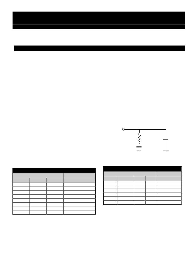
- This is the control output for the clock generator.
It is a single-ended, tri-state output. Component
connections are shown in Figure 1.
PRCLK FREQUENCY SELECTION
Inputs
TEST
S1
0
0
0
0
0
1
0
1
1
0
1
0
1
1
1
1
TABLE 1
: When Power Down address is slected, the
VCO is turned off and the device goes to standby
mode. Phase detector is in tri-state mode.
Output
PRCLK
9.96 Mhz
19.92 Mhz
24.9 Mhz
49.80 Mhz
0; Power Down
1; Power Down
TEST
Hi-Z
S0
0
1
0
1
0
1
0
1
MPCLK
- This is a nonmodulated output. This output
can be programmed to be 3.7 Mhz or 11.06 mHz. The
selection of these frequencies are controlled by the
MPSEL pin shown in Table 1.
PRCLK
- Output from the spectrum spread clock
generator. Frequency selection is shown on Table 1.
When the SSON pin is high, outputs are not
modulated. When SSON is low, sprectrum spread
function is enabled.
VSS
- Circuit ground
VDD
- Positive power supply
AVSS
- Analog circuit ground
AVDD
- Analog positive power supply
Figure 1
MPCLK FREQUENCY SELECTION
Inputs
TEST
MPSEL
S1
0
0
X
0
1
X
1
X
0
1
X
0
1
X
1
1
X
1
TABLE 2
: When Power Down address is selected, the
VCO is turned off and the device goes to standby
mode. Phase detector is in tri-state mode.
Output
PRCLK
3.7 Mhz
11.06 MHz
0; Power Down
1; Power Down
TEST
Hi-Z
S0
X
X
0
1
0
1
2k
2200 pf
R2
C2
330 pf
C1
相關(guān)PDF資料 |
PDF描述 |
|---|---|
| IMISG501XB | CPU System Clock Generator |
| IMISG502PB | CPU System Clock Generator |
| IMISG502PX | CPU System Clock Generator |
| IMISG508APB | Miscellaneous Clock Generator |
| IMISG508AXB | Miscellaneous Clock Generator |
相關(guān)代理商/技術(shù)參數(shù) |
參數(shù)描述 |
|---|---|
| IMISG501XB | 制造商:未知廠家 制造商全稱:未知廠家 功能描述:CPU System Clock Generator |
| IMISG502PB | 制造商:未知廠家 制造商全稱:未知廠家 功能描述:CPU System Clock Generator |
| IMISG502PX | 制造商:未知廠家 制造商全稱:未知廠家 功能描述:CPU System Clock Generator |
| IMISG508APB | 制造商:未知廠家 制造商全稱:未知廠家 功能描述:Miscellaneous Clock Generator |
| IMISG508AXB | 制造商:未知廠家 制造商全稱:未知廠家 功能描述:Miscellaneous Clock Generator |
發(fā)布緊急采購(gòu),3分鐘左右您將得到回復(fù)。