- 您現(xiàn)在的位置:買(mǎi)賣(mài)IC網(wǎng) > PDF目錄360850 > IMIC9531 Clocks and Buffers PDF資料下載
參數(shù)資料
| 型號(hào): | IMIC9531 |
| 英文描述: | Clocks and Buffers |
| 中文描述: | 時(shí)鐘和緩沖器 |
| 文件頁(yè)數(shù): | 3/10頁(yè) |
| 文件大小: | 125K |
| 代理商: | IMIC9531 |
C9530
Document #: 38-07033 Rev. *B
Page 3 of 10
Serial Data Interface
To enhance the flexibility and function of the clock synthesizer,
a two-signal serial interface is provided. Through the Serial
Data Interface, various device functions, such as individual
clock output buffers, can be individually enabled or disabled.
The registers associated with the Serial Data Interface
initializes to their default setting upon power-up, and therefore
use of this interface is optional. Clock device register changes
are normally made upon system initialization, if any are
required.
Data Protocol
The clock driver serial protocol accepts block write a opera-
tions from the controller. The bytes must be accessed in
sequential order from lowest to highest byte (most significant
bit first) with the ability to stop after any complete byte has
been transferred. The C9530 does not support the Block Read
function.
The block write protocol is outlined in
Table 2
. The addresses
are listed in
Table 3
.
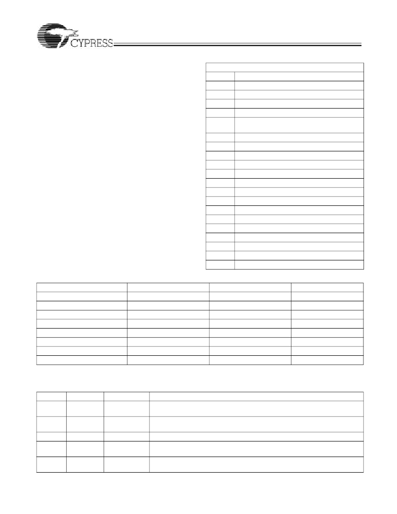
Table 2. Block Read and Block Write Protocol
Serial Control Registers
Block Write Protocol
Description
Bit
1
2:8
9
10
11:18
Start
Slave address – 7 bits
Write = 0
Acknowledge from slave
Command Code – 8 bits
‘00000000’ stands for block operation
Acknowledge from slave
Byte Count – 8 bits
Acknowledge from slave
Data byte 1 – 8 bits
Acknowledge from slave
Data byte 2 – 8 bits
Acknowledge from slave
......................
Data Byte (N–1) – 8 bits
Acknowledge from slave
Data Byte N – 8 bits
Acknowledge from slave
Stop
19
20:27
28
29:36
37
38:45
46
....
....
....
....
....
....
Table 3. SMBus Address Selection Table
SMBus Address of the Device
DE
DC
DA
D8
D6
D4
D0
D2
IA0 Bit (Pin 10)
0
1
0
1
0
1
0
1
IA1 Bit (Pin 11)
0
0
1
1
0
0
1
1
IA2 Bit (Pin 12)
0
0
0
0
1
1
1
1
Byte 0: Function Select Register
Bit
7
@Pup
1
Name
TESTEN
Description
Test Mode Enable.
1 = Normal operation, 0 = Test mode
Spread Spectrum modulation control bit (effective only when Bit 0 of this register is
set to a 0) 0 = OFF, 1= ON
SSCG Spread width select. 1 = 0.5%, 0 = 1.0% See
Table 4
below for clarification
SB1 Bank MSB frequency control bit (effective only when Bit 0 of this register is set
to a 0)
SB0 Bank LSB frequency control bit (effective only when Bit 0 of this register is set
to a 0)
6
0
SSEN
5
4
1
0
SSSEL
S1
3
0
S0
相關(guān)PDF資料 |
PDF描述 |
|---|---|
| IMIC9630 | Clocks and Buffers |
| IMIC9827H | Clocks and Buffers |
| IMIC9850A | Clocks and Buffers |
| IMIC9870G | Clocks and Buffers |
| IMIC9950 | Clocks and Buffers |
相關(guān)代理商/技術(shù)參數(shù) |
參數(shù)描述 |
|---|---|
| IMIC9531CT | 制造商:CYPRESS 制造商全稱(chēng):Cypress Semiconductor 功能描述:PCIX I/O System Clock Generator with EMI Control Features |
| IMIC9531CTT | 制造商:Cypress Semiconductor 功能描述: |
| IMIC9531CY | 制造商:Cypress Semiconductor 功能描述: |
| IMIC9531CYT | 制造商:Cypress Semiconductor 功能描述: |
| IMIC9630 | 制造商:未知廠家 制造商全稱(chēng):未知廠家 功能描述:Clocks and Buffers |
發(fā)布緊急采購(gòu),3分鐘左右您將得到回復(fù)。