- 您現(xiàn)在的位置:買賣IC網 > PDF目錄379217 > ILC6380BP-33 (Impala Linear Corporation) SOT-89 STEP-UP DUAL-MODE SWITCHER WITH SHUTDOWN PDF資料下載
參數資料
| 型號: | ILC6380BP-33 |
| 廠商: | Impala Linear Corporation |
| 英文描述: | SOT-89 STEP-UP DUAL-MODE SWITCHER WITH SHUTDOWN |
| 中文描述: | 采用SOT - 89 -向上雙路降壓模式可關斷開關 |
| 文件頁數: | 3/6頁 |
| 文件大小: | 186K |
| 代理商: | ILC6380BP-33 |
SOT-89 Step-up Dual-Mode Switcher with Shutdown
Impala Linear Corporation
3
(408) 574-3939
www.impalalinear.com
Sept 1999
ILC6380/1 1.4
V
OUT
= 5.0V, F
OSC
= 100kHz T
A
= 25°C. Unless otherwise specified, V
IN
= V
OUT
X0.6, I
OUT
= 50mA. See the schematic, figure 4.
Parameter
Symbol
Output Voltage
V
OUT
Test Circuit of Figure 2
Input Voltage
V
IN
Oscillation Startup Voltage
V
ST2
V
OUT
= V
ST2
Operation Startup Voltage
V
ST1
I
OUT
= 1mA
Supply Current 1
(See Note 2)
V
OUT
= 4.5V
Supply Current 2
I
DD
2
EXT = 10k
pull-up to 5V,
V
OUT
= 5.5V
EXT “High” On-Resistance
R
EXTH
EXT = 10k
pull-up to 5V,
V
OUT
= 4.5V, V
EXT
=
V
OUT
– 0.4V
EXT “Low” On-Resistance
R
EXTL
EXT = 10
pull-up to 5V,
V
OUT
= 4.5V, V
EXT
= V
OUT
- 0.4V
Oscillator Frequency
F
OSC
EXT = 10k
pull-up to 5V, V
OUT
=
4.5V, Measuring of EXT waveform
Maximum Duty Ratio
MAXDTY EXT = 10k
pull-up to 5V, V
OUT
=
4.5V, Measuring of EXT high state
CE “High” Voltage
V
CEH
EXT = 10k
pull-up to 5V, V
OUT
=
4.5V, Existence of Oscillation
CE “Low” Voltage
V
CEL
EXT = 10k
pull-up to 5V, V
OUT
=
4.5V, Stopped EXT Oscillation
CE “High” Current
I
CEH
EXT: 10k
pull-up to 5V,
V
OUT
= 4.5V, V
CE
= V
OUT
X 0.95V
CE “Low” Current
I
CEL
EXT = 10k
pull-up to 5V,
V
OUT
= 4.5V, V
CE
= 0V
Efficiency
EFFI
Slow Start Time
T
SS
Notes:
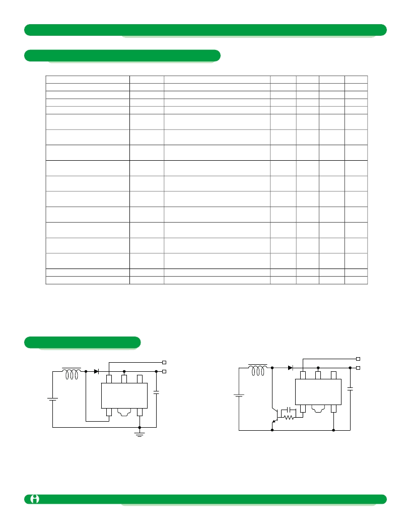
ILC6380
1
2
3
4
5
CE
V
OUT
C
L
+
GND
V
IN
L
SD
ILC6381
1
2
3
4
5
CE
V
OUT
C
L
+
L
SD
V
IN
C
B
R
B
Tr
L: 100μH ( SUMIDA, CD-54)
SD: Diode (Schottky diode; MATSUSHITA MA735)
CL: 16V 47μF (Tantalum Capacitor; NICHICON, F93)
L: 47μH ( SUMIDA, CD-54)
SD: Diode (Schottky diode; MATSUSHITA MA735)
CL: 16V 47μF (Tantalum Capacitor; NICHICON, F93)
RB: 1kW
CB: 3300pF
Tr: 2SC3279, 2SDI628G
Conditions
Min
4.875
Typ
5.000
78.6
Max
5.125
10
0.8
0.9
131.1
Units
V
V
V
V
μA
I
DD
1
EXT = 10k
pull-up to 5V,
6.9
13.8
μA
30
50
30
50
85
100
115
kHz
80
87
92
%
0.75
V
0.20
V
0.25
μA
-0.25
μA
85
10
%
msec
1. The Schottky diode (S.D.), in figure 3 must be type MA735, with Reverse current (IR) < 1.0μA at reverse voltage (VR)=10.0V
2. “Supply Current 1” is the supply current while the oscillator is continuously oscillating. In actual operation the oscillator periodically
operates which results in less average power consumption.
The current that is actually provided by external V
IN
source is represented by “No-Load Input Current (I
IN
)”
Electrical Characteristics ILC6380BP-50
Typical Applications
Figure 3
Figure 4
相關PDF資料 |
PDF描述 |
|---|---|
| ILC6380BP-50 | SOT-89 STEP-UP DUAL-MODE SWITCHER WITH SHUTDOWN |
| ILC6380CP-25 | SOT-89 STEP-UP DUAL-MODE SWITCHER WITH SHUTDOWN |
| ILC6380CP-33 | SOT-89 STEP-UP DUAL-MODE SWITCHER WITH SHUTDOWN |
| ILC6380CP-50 | SOT-89 STEP-UP DUAL-MODE SWITCHER WITH SHUTDOWN |
| ILC6380 | SOT-89 STEP-UP DUAL-MODE SWITCHER WITH SHUTDOWN |
相關代理商/技術參數 |
參數描述 |
|---|---|
| ILC6380BP33X | 功能描述:直流/直流開關轉換器 RoHS:否 制造商:STMicroelectronics 最大輸入電壓:4.5 V 開關頻率:1.5 MHz 輸出電壓:4.6 V 輸出電流:250 mA 輸出端數量:2 最大工作溫度:+ 85 C 安裝風格:SMD/SMT |
| ILC6380BP-50 | 制造商:Rochester Electronics LLC 功能描述:- Bulk |
| ILC6380BP50X | 功能描述:直流/直流開關轉換器 RoHS:否 制造商:STMicroelectronics 最大輸入電壓:4.5 V 開關頻率:1.5 MHz 輸出電壓:4.6 V 輸出電流:250 mA 輸出端數量:2 最大工作溫度:+ 85 C 安裝風格:SMD/SMT |
| ILC6380CP-25 | 制造商:Rochester Electronics LLC 功能描述:- Bulk 制造商:Fairchild Semiconductor Corporation 功能描述: |
| ILC6380CP25X | 功能描述:直流/直流開關轉換器 RoHS:否 制造商:STMicroelectronics 最大輸入電壓:4.5 V 開關頻率:1.5 MHz 輸出電壓:4.6 V 輸出電流:250 mA 輸出端數量:2 最大工作溫度:+ 85 C 安裝風格:SMD/SMT |
發(fā)布緊急采購,3分鐘左右您將得到回復。