- 您現(xiàn)在的位置:買賣IC網(wǎng) > PDF目錄9968 > IDT72V3652L15PF (IDT, Integrated Device Technology Inc)IC BI FIFO 4096X36 15NS 120QFP PDF資料下載
參數(shù)資料
| 型號(hào): | IDT72V3652L15PF |
| 廠商: | IDT, Integrated Device Technology Inc |
| 文件頁(yè)數(shù): | 24/29頁(yè) |
| 文件大?。?/td> | 0K |
| 描述: | IC BI FIFO 4096X36 15NS 120QFP |
| 標(biāo)準(zhǔn)包裝: | 45 |
| 系列: | 72V |
| 功能: | 異步,同步 |
| 存儲(chǔ)容量: | 147K(4K x 36) |
| 數(shù)據(jù)速率: | 67MHz |
| 訪問時(shí)間: | 15ns |
| 電源電壓: | 3.15 V ~ 3.45 V |
| 工作溫度: | 0°C ~ 70°C |
| 安裝類型: | 表面貼裝 |
| 封裝/外殼: | 120-LQFP |
| 供應(yīng)商設(shè)備封裝: | 120-TQFP(14x14) |
| 包裝: | 托盤 |
| 其它名稱: | 72V3652L15PF |
第1頁(yè)第2頁(yè)第3頁(yè)第4頁(yè)第5頁(yè)第6頁(yè)第7頁(yè)第8頁(yè)第9頁(yè)第10頁(yè)第11頁(yè)第12頁(yè)第13頁(yè)第14頁(yè)第15頁(yè)第16頁(yè)第17頁(yè)第18頁(yè)第19頁(yè)第20頁(yè)第21頁(yè)第22頁(yè)第23頁(yè)當(dāng)前第24頁(yè)第25頁(yè)第26頁(yè)第27頁(yè)第28頁(yè)第29頁(yè)
4
COMMERCIALTEMPERATURERANGE
IDT72V3652/72V3662/72V3672 3.3V CMOS SyncBiFIFOTM
2,048 x 36 x 2, 4,096 x 36 x 2 and 8,192 x 36 x 2
FEBRUARY 4, 2009
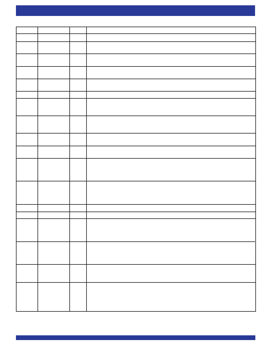
Symbol
Name
I/O
Description
A0-A35
Port A Data
I/0
36-bit bidirectional data port for side A.
AEA
Port A Almost-
O
Programmable Almost-Empty flag synchronized to CLKA. It is LOW when the number of words in FIFO2 is
Empty Flag
(Port A)
less than or equal to the value in the Almost-Empty A Offset register, X2.
AEB
Port B Almost-
O
Programmable Almost-Empty flag synchronized to CLKB. It is LOW when the number of words in FIFO1 is
Empty Flag
(Port B)
less than or equal to the value in the Almost-Empty B Offset register, X1.
AFA
Port A Almost-
O
Programmable Almost-Full flag synchronized to CLKA. It is LOW when the number of empty locations in
Full Flag
(Port A)
FIFO1 is less than or equal to the value in the Almost-Full A Offset register, Y1.
AFB
Port B Almost-
O
Programmable Almost-Full flag synchronized to CLKB. It is LOW when the number of empty locations in
Full Flag
(Port B)
FIFO2 is less than or equal to the value in the Almost-Full B Offset register, Y2.
B0 - B35
Port B Data
I/O
36-bit bidirectional data port for side B.
CLKA
Port A Clock
I
CLKA is a continuous clock that synchronizes all data transfers through port A and can be asynchronous or
coincident to CLKB.
FFA/IRA, EFA/ORA, AFA, and AEA are all synchronized to the LOW-to-HIGH
transition of CLKA.
CLKB
Port B Clock
I
CLKB is a continuous clock that synchronizes all data transfers through port Band can be asynchronous or
coincident to CLKA.
FFB/IRB, EFB/ORB, AFB, and AEB are synchronized to the LOW-to-HIGH
transition of CLKB.
CSA
Port A Chip
I
CSA must be LOW to enable a LOW-to-HIGH transition of CLKA to read or write on port A. The A0-A35
Select
outputs are in the high-impedance state when
CSA is HIGH.
CSB
Port B Chip
I
CSB must be LOW to enable a LOW-to-HIGH transition of CLKB to read or write data on port B. The
Select
B0- B35 outputs are in the high-impedance state when
CSB is HIGH.
EFA/ORA
Port A Empty/
O
This is a dual function pin. In the IDT Standard mode, the
EFA function is selected. EFA indicates
Output Ready
whether or not the FIFO2 memory is empty. In the FWFT mode, the ORA function is selected. ORA
Flag
indicates the presence of valid data on A0-A35 outputs, available for reading.
EFA/ORA is synchronized
to the LOW-to-HIGH transition of CLKA.
EFB/ORB
Port B Empty/
O
This is a dual function pin. In the IDT Standard mode, the
EFB function is selected. EFB indicates
Output Ready
whether or not the FIFO1 memory is empty. In the FWFT mode, the ORB function is selected. ORB
Flag
indicates the presence of valid data on B0-B35 outputs, available for reading.
EFB/ORB is synchronized to
the LOW-to-HIGH transition of CLKB.
ENA
Port A Enable
I
ENA must be HIGH to enable a LOW-to-HIGH transition of CLKA to read or write data on port A.
ENB
Port B Enable
I
ENB must be HIGH to enable a LOW-to-HIGH transition of CLKB to read or write data on port B.
FFA/IRA
Port A Full/
O
This is a dual function pin. In the IDT Standard mode, the
FFA function is selected. FFA indicates
Input Ready
whether or not the FIFO1 memory is full. In the FWFT mode, the IRA function is selected. IRA
Flag
indicates whether or not there is space available for writing to the FIFO1 memory.
FFA/IRA is
synchronized to the LOW-to-HIGH transition of CLKA.
FFB/IRB
Port B Full/
O
This is a dual function pin. In the IDT Standard mode, the
FFB function is selected. FFB indicates
Input Ready
whether or not the FIFO2 memory is full. In the FWFT mode, the IRB function is selected. IRB
Flag
indicates whether or not there is space available for writing to the FIFO2 memory.
FFB/IRB is
synchronized to the LOW-to-HIGH transition of CLKB.
FWFT
First Word Fall
I
This pin selects the timing mode. A HIGH on
FWFT selects IDT Standard mode, a LOW selects First
Through Mode
Word Fall Through mode. Once the timing mode has been selected, the level on
FWFT must be static
throughout device operation.
FS1, FS0
FlagOffset
I
A LOW-to-HIGH transition of the FIFO Reset input latches the values of FS0 and FS1. If either FS0 or
Selects
FS1 is HIGH when the FIFO Reset input goes HIGH, one of three preset values is selected as the
offset for FIFOs Almost-Full and Almost-Empty flags. If both FIFOs are reset simultaneously and both
FS0 and FS1 are LOW when
RST1 and RST2 go HIGH, the first four writes to FIFO1 load the Almost-
Empty and Almost-Full offsets for both FIFOs.
PIN DESCRIPTIONS
相關(guān)PDF資料 |
PDF描述 |
|---|---|
| IDT82V2088DR | IC LIU T1/J1/E1 8CH 208-TQFP |
| VE-B6Z-IU-F2 | CONVERTER MOD DC/DC 2V 80W |
| VI-21J-MX-F2 | CONVERTER MOD DC/DC 36V 75W |
| VE-B6Z-IU-F1 | CONVERTER MOD DC/DC 2V 80W |
| V48B15M250BG3 | CONVERTER MOD DC/DC 15V 250W |
相關(guān)代理商/技術(shù)參數(shù) |
參數(shù)描述 |
|---|---|
| IDT72V3652L15PF8 | 功能描述:IC BI FIFO 4096X36 15NS 120QFP RoHS:否 類別:集成電路 (IC) >> 邏輯 - FIFO 系列:72V 標(biāo)準(zhǔn)包裝:90 系列:7200 功能:同步 存儲(chǔ)容量:288K(16K x 18) 數(shù)據(jù)速率:100MHz 訪問時(shí)間:10ns 電源電壓:4.5 V ~ 5.5 V 工作溫度:0°C ~ 70°C 安裝類型:表面貼裝 封裝/外殼:64-LQFP 供應(yīng)商設(shè)備封裝:64-TQFP(14x14) 包裝:托盤 其它名稱:72271LA10PF |
| IDT72V3652L15PQF | 功能描述:IC BI FIFO 4096X36 15NS 132QFP RoHS:否 類別:集成電路 (IC) >> 邏輯 - FIFO 系列:72V 標(biāo)準(zhǔn)包裝:90 系列:7200 功能:同步 存儲(chǔ)容量:288K(16K x 18) 數(shù)據(jù)速率:100MHz 訪問時(shí)間:10ns 電源電壓:4.5 V ~ 5.5 V 工作溫度:0°C ~ 70°C 安裝類型:表面貼裝 封裝/外殼:64-LQFP 供應(yīng)商設(shè)備封裝:64-TQFP(14x14) 包裝:托盤 其它名稱:72271LA10PF |
| IDT72V3653L10PF | 功能描述:IC SYNCFIFO 2048X36 10NS 128TQFP RoHS:否 類別:集成電路 (IC) >> 邏輯 - FIFO 系列:72V 標(biāo)準(zhǔn)包裝:90 系列:7200 功能:同步 存儲(chǔ)容量:288K(16K x 18) 數(shù)據(jù)速率:100MHz 訪問時(shí)間:10ns 電源電壓:4.5 V ~ 5.5 V 工作溫度:0°C ~ 70°C 安裝類型:表面貼裝 封裝/外殼:64-LQFP 供應(yīng)商設(shè)備封裝:64-TQFP(14x14) 包裝:托盤 其它名稱:72271LA10PF |
| IDT72V3653L10PF8 | 功能描述:IC SYNCFIFO 2048X36 10NS 128TQFP RoHS:否 類別:集成電路 (IC) >> 邏輯 - FIFO 系列:72V 標(biāo)準(zhǔn)包裝:90 系列:7200 功能:同步 存儲(chǔ)容量:288K(16K x 18) 數(shù)據(jù)速率:100MHz 訪問時(shí)間:10ns 電源電壓:4.5 V ~ 5.5 V 工作溫度:0°C ~ 70°C 安裝類型:表面貼裝 封裝/外殼:64-LQFP 供應(yīng)商設(shè)備封裝:64-TQFP(14x14) 包裝:托盤 其它名稱:72271LA10PF |
| IDT72V3653L15PF | 功能描述:IC SYNCFIFO 2048X36 15NS 128TQFP RoHS:否 類別:集成電路 (IC) >> 邏輯 - FIFO 系列:72V 標(biāo)準(zhǔn)包裝:90 系列:7200 功能:同步 存儲(chǔ)容量:288K(16K x 18) 數(shù)據(jù)速率:100MHz 訪問時(shí)間:10ns 電源電壓:4.5 V ~ 5.5 V 工作溫度:0°C ~ 70°C 安裝類型:表面貼裝 封裝/外殼:64-LQFP 供應(yīng)商設(shè)備封裝:64-TQFP(14x14) 包裝:托盤 其它名稱:72271LA10PF |
發(fā)布緊急采購(gòu),3分鐘左右您將得到回復(fù)。