- 您現(xiàn)在的位置:買賣IC網(wǎng) > PDF目錄377422 > IDT72841L20PF (INTEGRATED DEVICE TECHNOLOGY INC) DUAL CMOS SyncFIFO PDF資料下載
參數(shù)資料
| 型號(hào): | IDT72841L20PF |
| 廠商: | INTEGRATED DEVICE TECHNOLOGY INC |
| 元件分類: | DRAM |
| 英文描述: | DUAL CMOS SyncFIFO |
| 中文描述: | 8K X 9 BI-DIRECTIONAL FIFO, PQFP64 |
| 封裝: | 14 X 14 MM, 1.40 MM HEIGHT, TQFP-64 |
| 文件頁(yè)數(shù): | 3/21頁(yè) |
| 文件大小: | 228K |
| 代理商: | IDT72841L20PF |
第1頁(yè)第2頁(yè)當(dāng)前第3頁(yè)第4頁(yè)第5頁(yè)第6頁(yè)第7頁(yè)第8頁(yè)第9頁(yè)第10頁(yè)第11頁(yè)第12頁(yè)第13頁(yè)第14頁(yè)第15頁(yè)第16頁(yè)第17頁(yè)第18頁(yè)第19頁(yè)第20頁(yè)第21頁(yè)
5.15
3
COMMERCIAL TEMPERATURE
72801/72811/72821/72831/72841 DUAL CMOS SyncFIFO
256 x 9, 512 x 9, 1024 x 9, 2048 x 9 and 4096 x 9
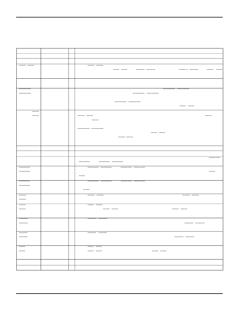
PIN DESCRIPTIONS
The 72801/72811/72821/72831/72841s two FIFOs, referred
to as FIFO A and FIFO B, are identical in every respect. The
following description defines the input and output signals for
FIFO A. The corresponding signal names for FIFO B are
provided in parentheses.
Symbol
D
A0
-D
A8
D
B0
-D
B8
RSA
,
RSB
Name I/O
A Data Inputs
B Data Inputs
Reset
Description
9-bit data inputs to RAM array A.
9-bit data inputs to RAM array B.
When
RSA
(
RSB
) is set LOW, the associated internal read and write pointers of array A (B) are
set to the first location;
FFA
(
FFB
) and
PAFA
(
PAFB
) go HIGH, and
PAEA
(
PAEB
) and
EFA
(
EFB
)
go LOW. After power-up, a reset of both FIFOs A and B is required before an initial WRITE.
Data is written into the FIFO A (B) on a LOW-to-HIGH transition of WCLKA (WCLKB) when the
write enable(s) are asserted.
If FIFO A (B) is configured to have programmable flags,
WENA1
(
WENB1
) is the only write
enable pin that can be used. When
WENA1
(
WENB1
) is LOW, data A (B) is written into the
FIFO on every LOW-to-HIGH transition WCLKA (WCLKB). If the FIFO is configured to
have two write enables,
WENA1
(
WENB1
) must be LOW and WENA2 (WENB2) must be HIGH
to write data into the FIFO. Data will not be written into the FIFO if
FFA
(
FFB
) is LOW.
FIFO A (B) is configured at reset to have either two write enables or programmable flags. If
LDA
(
LDB
) is HIGH at reset, this pin operates as a second write enable. If WENA2/
LDA
(WENB2/
LDB
) is LOW at reset this pin operates as a control to load and read the program
mable flag offsets for its respective array. If the FIFO is configured to have two write enables,
WENA1
(
WENB1
) must be LOW and WENA2 (WENB2) must be HIGH to write data into FIFO
A (B). Data will not be written into FIFO A (B) if
FFA
(
FFB
) is LOW. If the FIFO is configured to
have programmable flags,
LDA
(
LDB
) is held LOW to write or read the programmable flag
offsets.
9-bit data outputs from RAM array A.
9-bit data outputs from RAM array B.
Data is read from FIFO A (B) on a LOW-to-HIGH transition of RCLKA (RCLKB) when
RENA1
(
RENB1
) and
RENA2
(
RENB2
) are asserted.
When
RENA1
(
RENB1
) and
RENA2
(
RENB2
) are LOW, data is read from FIFO A (B) on every
LOW-to-HIGH transition of RCLKA (RCLKB). Data will not be read from Array A (B) if
EFA
(
EFB
) is LOW.
When
RENA1
(
RENB1
) and
RENA2
(
RENB2
) are LOW, data is read from the FIFO A (B) on
every LOW-to-HIGH transition of RCLKA (RCLKB). Data will not be read from array A (B) if
the
EFA
(EFB) is LOW.
When
OEA
(
OEB
) is LOW, outputs D
A0
-D
A8
(D
B0
-D
B8
) are active. If
OEA
(
OEB
) is HIGH, the
outputs D
A0
-D
A8
(D
B0
-D
B8
) will be in a high-impedance state.
When
EFA
(
EFB
) is LOW, FIFO A (B) is empty and further data reads from the output are
inhibited. When
EFA
(
EFB
) is HIGH, FIFO A (B) is not empty.
EFA
(
EFB
) is synchronized to
RCLKA (RCLKB).
When
PAEA
(
PAEB
) is LOW, FIFO A (B) is almost empty based on the offset programmed into
the appropriate offset register. The default offset at reset is Empty+7.
PAEA
(
PAEB
) is synchro
nized to RCLKA (RCLKB).
When
PAFA
(
PAFB
) is LOW, FIFO A (B) is almost full based on the offset programmed into the
appropriate offset register. The default offset at reset is Full-7.
PAFA
(
PAFB
) is synchronized
to WCLKA (WCLKB).
When
FFA
(
FFB
) is LOW, FIFO A (B) is full and further data writes into the input are inhibited.
When
FFA
(
FFB
) is HIGH, FIFO A (B) is not full.
FFA
(
FFB
) is synchronized to WCLKA
(WCLKB).
+5V power supply pin.
0V ground pin.
I
I
I
WCLKA
WCLKB
WENA1
WENB1
Write Clock
I
Write Enable 1
I
WENA2/
LDA
WENB2/
LDB
Write Enable 2/
Load
I
Q
A0
-Q
A8
Q
B0
-Q
B8
RCLKA
RCLKB
RENA1
RENB1
A Data Outputs O
B Data Outputs O
Read Clock
I
Read Enable 1
I
RENA2
RENB2
Read Enable 2
I
OEA
OEB
EFA
EFB
Output Enable
I
Empty Flag
O
PAEA
PAEB
Programmable
Almost-Empty
Flag
Programmable
Almost-Full Flag
O
PAFA
PAFB
O
FFA
FFB
Full Flag
O
V
CC
GND
Power
Ground
3034 tbl 01
相關(guān)PDF資料 |
PDF描述 |
|---|---|
| IDT72841L25PF | DUAL CMOS SyncFIFO |
| IDT72841L35PF | DUAL CMOS SyncFIFO |
| IDT72801L12PF | DUAL CMOS SyncFIFO |
| IDT72801L15PF | DUAL CMOS SyncFIFO |
| IDT72801L20PF | DUAL CMOS SyncFIFO |
相關(guān)代理商/技術(shù)參數(shù) |
參數(shù)描述 |
|---|---|
| IDT72841L25PF | 功能描述:IC FIFO SYNC 4KX9 25NS 64QFP RoHS:否 類別:集成電路 (IC) >> 邏輯 - FIFO 系列:7200 標(biāo)準(zhǔn)包裝:90 系列:7200 功能:同步 存儲(chǔ)容量:288K(16K x 18) 數(shù)據(jù)速率:100MHz 訪問(wèn)時(shí)間:10ns 電源電壓:4.5 V ~ 5.5 V 工作溫度:0°C ~ 70°C 安裝類型:表面貼裝 封裝/外殼:64-LQFP 供應(yīng)商設(shè)備封裝:64-TQFP(14x14) 包裝:托盤 其它名稱:72271LA10PF |
| IDT72841L25PF8 | 功能描述:IC FIFO SYNC 4KX9 25NS 64QFP RoHS:否 類別:集成電路 (IC) >> 邏輯 - FIFO 系列:7200 標(biāo)準(zhǔn)包裝:90 系列:7200 功能:同步 存儲(chǔ)容量:288K(16K x 18) 數(shù)據(jù)速率:100MHz 訪問(wèn)時(shí)間:10ns 電源電壓:4.5 V ~ 5.5 V 工作溫度:0°C ~ 70°C 安裝類型:表面貼裝 封裝/外殼:64-LQFP 供應(yīng)商設(shè)備封裝:64-TQFP(14x14) 包裝:托盤 其它名稱:72271LA10PF |
| IDT72841L25PFI | 功能描述:IC FIFO SYNC 4KX9 25NS 64QFP RoHS:否 類別:集成電路 (IC) >> 邏輯 - FIFO 系列:7200 標(biāo)準(zhǔn)包裝:90 系列:7200 功能:同步 存儲(chǔ)容量:288K(16K x 18) 數(shù)據(jù)速率:100MHz 訪問(wèn)時(shí)間:10ns 電源電壓:4.5 V ~ 5.5 V 工作溫度:0°C ~ 70°C 安裝類型:表面貼裝 封裝/外殼:64-LQFP 供應(yīng)商設(shè)備封裝:64-TQFP(14x14) 包裝:托盤 其它名稱:72271LA10PF |
| IDT72841L25PFI8 | 功能描述:IC FIFO SYNC 4KX9 25NS 64QFP RoHS:否 類別:集成電路 (IC) >> 邏輯 - FIFO 系列:7200 標(biāo)準(zhǔn)包裝:90 系列:7200 功能:同步 存儲(chǔ)容量:288K(16K x 18) 數(shù)據(jù)速率:100MHz 訪問(wèn)時(shí)間:10ns 電源電壓:4.5 V ~ 5.5 V 工作溫度:0°C ~ 70°C 安裝類型:表面貼裝 封裝/外殼:64-LQFP 供應(yīng)商設(shè)備封裝:64-TQFP(14x14) 包裝:托盤 其它名稱:72271LA10PF |
| IDT72841L25TF | 功能描述:IC FIFO SYNC 4KX9 25NS 64QFP RoHS:否 類別:集成電路 (IC) >> 邏輯 - FIFO 系列:7200 標(biāo)準(zhǔn)包裝:90 系列:7200 功能:同步 存儲(chǔ)容量:288K(16K x 18) 數(shù)據(jù)速率:100MHz 訪問(wèn)時(shí)間:10ns 電源電壓:4.5 V ~ 5.5 V 工作溫度:0°C ~ 70°C 安裝類型:表面貼裝 封裝/外殼:64-LQFP 供應(yīng)商設(shè)備封裝:64-TQFP(14x14) 包裝:托盤 其它名稱:72271LA10PF |
發(fā)布緊急采購(gòu),3分鐘左右您將得到回復(fù)。