- 您現(xiàn)在的位置:買賣IC網(wǎng) > PDF目錄377421 > IDT72605L20PF (INTEGRATED DEVICE TECHNOLOGY INC) CMOS SyncBiFIFOO 256 x 18 x 2 and 512 x 18 x 2 PDF資料下載
參數(shù)資料
| 型號: | IDT72605L20PF |
| 廠商: | INTEGRATED DEVICE TECHNOLOGY INC |
| 元件分類: | DRAM |
| 英文描述: | CMOS SyncBiFIFOO 256 x 18 x 2 and 512 x 18 x 2 |
| 中文描述: | 256 X 18 BI-DIRECTIONAL FIFO, 10 ns, PQFP64 |
| 封裝: | TQFP-64 |
| 文件頁數(shù): | 8/20頁 |
| 文件大小: | 209K |
| 代理商: | IDT72605L20PF |
IDT72605/IDT72615 CMOS SyncBiFIFO
256 x 18 x 2 and 512 x 18 x 2
COMMERCIAL TEMPERATURE RANGE
5.18
8
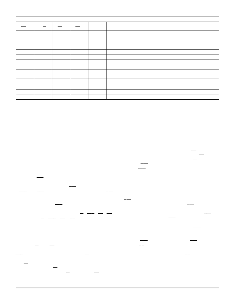
Data A
I/O
I
CS
A
0
R/
W
A
0
EN
A
0
OE
A
0
Port A Operation
Data A is written on CLKA
≠
. This write cycle immediately following
low-impedance cycle is prohibited. Note that even though OE
A
= 0, a
LOW logic level on R/W
A
, once qualified by a rising edge on CLK
A,
will
put Data A into a high-impedance state.
Data A is written on CLKA
≠
Data A is ignored
Data is read
(1)
from RAM array to output register on CLKA
≠
,
Data A is low-impedance
Data is read
(1)
from RAM array to output register on CLKA
≠
,
Data A is high-impedance
Output register does not change
(2)
, Data A is low-impedance
Output register does not change
(2)
, Data A is high-impedance
Data A is ignored
(3)
Data A is high-impedance
(3)
0
0
0
0
0
1
0
1
0
1
X
0
I
I
O
0
1
0
1
O
0
0
1
1
1
1
0
1
1
1
X
X
0
1
X
X
O
O
I
O
NOTES:
1. When A
2
A
1
A
0
= 000, the next B
→
A FIFO value is read out of the output register and the read pointer advances. If A
2
A
1
A
0
= 001, the bypass path is
selected and bypass data from the Port B input register is read from the Port A output register. If A
2
A
1
A
0
0 = 1XX, a flag offset register is selected
and its offset is read out through Port A output register.
2. Regardless of the condition of A
2
A
1
A
0
, the data in the Port A output register does not change and the B
→
A read pointer does not advance.
3. If CS
A#
is HIGH, then BYP
B
is HIGH. No bypass occur under this condition.
2704 tbl 09
BYPASS PATH
The bypass paths provide direct communication between
Port A and Port B. There are two full 18-bit bypass paths, one
in each direction. During a bypass operation, data is passed
directly between the input and output registers, and the FIFO
memory is undisturbed.
Port A initiates and terminates all bypass operations. The
bypass flag,
BYP
B
, is asserted to inform Port B that a bypass
operation is beginning. The bypass flag state is controlled by
the Port A controls, although the
BYP
B
signal is synchronized
to
CLK
B
. So,
BYP
B
is asserted on the next rising edge of
CLK
B
when A
2
A
1
A
0
=001and CS
A
is LOW. When Port A returns to
normal FIFO mode (A
2
A
1
A
0
=000 or CS
A
is HIGH),
BYP
B
is
deasserted on the next
CLK
B
rising edge.
Once the SyncBiFIFO is in bypass mode, all data transfers
are controlled by the standard Port A (R/
W
A
,
CLK
A
,
EN
A
,
OE
A
)
and Port B (R/
W
B
,
CLK
B
,
EN
B
,
OE
B
) interface pins. Each
bypass path can be considered as a one word deep FIFO.
Data is held in each input register until it is read. Since the
controls of each port operate independently, Port A can be
reading bypass data at the same time Port B is reading bypass
data.
When R/
W
A
and
EN
A
is LOW, data on pins D
A0
-D
A17
is
written into Port A input register. Following the rising edge of
CLK
A
for this write, the A
→
B Full Flag (
FF
AB
) goes LOW.
Subsequent writes into Port A are blocked by internal logic
until
FF
AB
goes HIGH again. On the next CLKB rising edge,
the A
→
B Empty Flag (
EF
AB
) goes HIGH indicating to Port B
that data is available. Once R/
W
B
is HIGH and
EN
B
is LOW,
data is read into the Port B output register.
OE
B
still controls
whether Port B is in a high-impedance state. When
OE
B
is LOW,
the output register data appears at D
B0
-D
B17
.
EF
AB
goes LOW
following the
CLK
B
rising edge for this read. FFAB goes HIGH
on the next
CLK
A
rising edge, letting Port A know that another
word can be written through the bypass path.
Bypass data transfers from Port B to Port A work in a similar
manner with
EFB
A
and
FFB
A
indicating the Port A output
register state.
When the Port A address changes from bypass mode
(A
2
A
1
A
0
=001) to FIFO mode (A
2
A
1
A
0
=000) on the rising edge
of
CLK
A
, the data held in the Port B output register may be
overwritten. Unless Port A monitors the
BYP
B
pin and waits
for Port B to clock out the last bypass word, data from the A
→
B
FIFO will overwrite data in the Port B output register.
BYP
B
will
go HIGH on the rising edge of
CLK
B
signifying that Port B has
finished its last bypass operation. Port B must read any
bypass data in the output register on this last
CLK
B
clock or it
is lost and the SyncBiFIFO returns to FIFO operations. It is
especially important to monitor
BYP
B
when
CLK
B
is much
slower than
CLK
A
to avoid this condition.
BYP
B
will also go
HIGH after
CS
A
is brought HIGH; in this manner the Port B
bypass data may also be lost.
Since the Port A processor controls
CS
A
and the bypass
mode, this scenario can be handled for B
→
A bypass data. The
Port A processor must be set up to read the last bypass word
before leaving bypass mode.
Table 1. Port A Operation Control Signals
相關(guān)PDF資料 |
PDF描述 |
|---|---|
| IDT72605L25G | Precision Micropower Shunt Voltage Reference 5-SC70 -40 to 85 |
| IDT72605L25J | CMOS SyncBiFIFOO 256 x 18 x 2 and 512 x 18 x 2 |
| IDT72605L25PF | CMOS SyncBiFIFOO 256 x 18 x 2 and 512 x 18 x 2 |
| IDT72605L35G | CMOS SyncBiFIFOO 256 x 18 x 2 and 512 x 18 x 2 |
| IDT72605L35J | CMOS SyncBiFIFOO 256 x 18 x 2 and 512 x 18 x 2 |
相關(guān)代理商/技術(shù)參數(shù) |
參數(shù)描述 |
|---|---|
| IDT72605L20PF8 | 功能描述:IC FIFO BI SYNC 256X18 64-TQFP RoHS:否 類別:集成電路 (IC) >> 邏輯 - FIFO 系列:7200 標(biāo)準(zhǔn)包裝:90 系列:7200 功能:同步 存儲容量:288K(16K x 18) 數(shù)據(jù)速率:100MHz 訪問時間:10ns 電源電壓:4.5 V ~ 5.5 V 工作溫度:0°C ~ 70°C 安裝類型:表面貼裝 封裝/外殼:64-LQFP 供應(yīng)商設(shè)備封裝:64-TQFP(14x14) 包裝:托盤 其它名稱:72271LA10PF |
| IDT72605L25J | 功能描述:IC FIFO BI SYNC 256X18 68-PLCC RoHS:否 類別:集成電路 (IC) >> 邏輯 - FIFO 系列:7200 標(biāo)準(zhǔn)包裝:90 系列:7200 功能:同步 存儲容量:288K(16K x 18) 數(shù)據(jù)速率:100MHz 訪問時間:10ns 電源電壓:4.5 V ~ 5.5 V 工作溫度:0°C ~ 70°C 安裝類型:表面貼裝 封裝/外殼:64-LQFP 供應(yīng)商設(shè)備封裝:64-TQFP(14x14) 包裝:托盤 其它名稱:72271LA10PF |
| IDT72605L25J8 | 功能描述:IC FIFO BI SYNC 256X18 68-PLCC RoHS:否 類別:集成電路 (IC) >> 邏輯 - FIFO 系列:7200 標(biāo)準(zhǔn)包裝:90 系列:7200 功能:同步 存儲容量:288K(16K x 18) 數(shù)據(jù)速率:100MHz 訪問時間:10ns 電源電壓:4.5 V ~ 5.5 V 工作溫度:0°C ~ 70°C 安裝類型:表面貼裝 封裝/外殼:64-LQFP 供應(yīng)商設(shè)備封裝:64-TQFP(14x14) 包裝:托盤 其它名稱:72271LA10PF |
| IDT72605L25PF | 功能描述:IC FIFO BI SYNC 256X18 64-TQFP RoHS:否 類別:集成電路 (IC) >> 邏輯 - FIFO 系列:7200 標(biāo)準(zhǔn)包裝:90 系列:7200 功能:同步 存儲容量:288K(16K x 18) 數(shù)據(jù)速率:100MHz 訪問時間:10ns 電源電壓:4.5 V ~ 5.5 V 工作溫度:0°C ~ 70°C 安裝類型:表面貼裝 封裝/外殼:64-LQFP 供應(yīng)商設(shè)備封裝:64-TQFP(14x14) 包裝:托盤 其它名稱:72271LA10PF |
| IDT72605L25PF8 | 功能描述:IC FIFO BI SYNC 256X18 64-TQFP RoHS:否 類別:集成電路 (IC) >> 邏輯 - FIFO 系列:7200 標(biāo)準(zhǔn)包裝:90 系列:7200 功能:同步 存儲容量:288K(16K x 18) 數(shù)據(jù)速率:100MHz 訪問時間:10ns 電源電壓:4.5 V ~ 5.5 V 工作溫度:0°C ~ 70°C 安裝類型:表面貼裝 封裝/外殼:64-LQFP 供應(yīng)商設(shè)備封裝:64-TQFP(14x14) 包裝:托盤 其它名稱:72271LA10PF |
發(fā)布緊急采購,3分鐘左右您將得到回復(fù)。