- 您現(xiàn)在的位置:買賣IC網(wǎng) > PDF目錄377274 > IDT7099S (Integrated Device Technology, Inc.) JFET-Input Operational Amplifier 8-PDIP 0 to 70 PDF資料下載
參數(shù)資料
| 型號: | IDT7099S |
| 廠商: | Integrated Device Technology, Inc. |
| 英文描述: | JFET-Input Operational Amplifier 8-PDIP 0 to 70 |
| 中文描述: | 高速4K的× 9同步雙端口RAM |
| 文件頁數(shù): | 8/9頁 |
| 文件大?。?/td> | 131K |
| 代理商: | IDT7099S |
6.23
8
IDT7099S
HIGH-SPEED 4K x 9 SYNCHRONOUS DUAL-PORT RAM
MILITARY AND COMMERCIAL TEMPERATURE RANGES
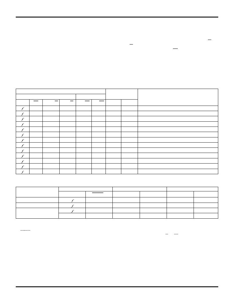
TRUTH TABLE I – READ/WRITE CONTROL
(1)
Inputs
Synchronous
(3)
Asynchronous
CLK
CE
Byte R/
W
h
h
h
l
h
h
h
l
l
l
l
l
l
h
l
h
l
l
l
h
l
h
l
h
l
h
Outputs
I/O0-7
High-Z
DATA
IN
High-Z
DATA
IN
DATA
IN
DATA
OUT
DATA
IN
DATA
OUT
DATA
IN
High-Z
DATA
IN
DATA
OUT
DATA
OUT
High-Z
DATA
OUT
High-Z
Bit R/
h
h
l
l
h
h
l
l
l
h
h
h
h
W
Byte
X
X
X
X
X
X
L
H
X
L
H
L
H
OE
Bit
X
X
X
X
L
H
X
X
X
L
L
H
H
OE
I/O8
High-Z
High-Z
DATA
IN
DATA
IN
Mode
Deselected, Power Down, Data I/O Disabled
Deselected, Power Down, Byte Data Input Enabled
Deselected, Power Down, Bit Data Input Enabled
Deselected, Power Down, Data Input Enabled
Write Byte, Read Bit
Write Byte Only
Read Byte, Write Bit
Write Bit Only
Write Byte, Write Bit
Read Byte, Read Bit
Read Bit Only
Read Byte Only
Data I/O Disabled
High-Z
DATA
IN
DATA
IN
DATA
OU
T
High-Z
High-Z
3007 tbl 09
FUNCTIONAL DESCRIPTION
The IDT7099 provides a true synchronous Dual-Port Static
RAM interface. Registered inputs provide very short set-up
and hold times on address, data, and all critical control inputs.
All internal registers are clocked on the rising edge of the clock
signal. An asynchronous output enable is provided to ease
asynchronous bus interfacing.
The internal write pulse width is dependent on the low to
high transitions of the clock signal allowing the shortest
possible realized cycle times. Clock enable inputs are
provided to stall the operation of the address and data input
registers without introducing clock skew for very fast inter-
leaved memory applications.
The data inputs are gated to control on-chip noise in bussed
applications. The user must guarantee that the BYTE R/
W
and
BIT R/
W
pins are low for at least one clock cycle before any
write is attempted. A High on the
CE
input for one clock cycle
will power down the internal circuitry to reduce static power
consumption.
The device has separate Bit Write, Byte Write, Bit Enable,
and Byte Enable pins to allow for independent control.
TRUTH TABLE II – CLOCK ENABLE FUNCTION TABLE
(1)
Inputs
Register Inputs
Register Outputs
Operating Mode
Load "1"
Load "0"
Hold (do nothing)
CLK
(3)
CLKEN
(2)
ADDR
h
l
X
X
DATAIN
h
l
X
X
ADDR
H
L
NC
NC
DATAOUT
H
L
NC
NC
l
l
h
H
X
NOTES:
1. 'H' = High voltage level steady state, 'h' = High voltage level one set-up time prior to the low-to-high clock transition, 'L' = Low voltage level steady state
'l' = Low voltage level one set-up time prior to the Low-to-High clock transition, 'X' = Don't care, 'NC' = No change
2.
CLKEN
= V
IL
must be clocked in during Power-Up.
3. Control signals are initialted and terminated on the rising edge of the CLK, depending on their input level. When R/
W
and
CE
are low, a write cycle is initiated
on the low-to-high transition of the CLK. Termination of a write cycle is done on the next low-to-high transistion of the CLK.
3007 tbl 10
相關PDF資料 |
PDF描述 |
|---|---|
| IDT7099S15G | JFET-Input Operational Amplifier 8-SO 0 to 70 |
| IDT7099S15GB | JFET-Input Operational Amplifier 8-SO 0 to 70 |
| IDT7099S15J | HIGH-SPEED 4K x 9 SYNCHRONOUS DUAL-PORT RAM |
| IDT7099S15JB | HIGH-SPEED 4K x 9 SYNCHRONOUS DUAL-PORT RAM |
| IDT7099S15PF | JFET-Input Operational Amplifier 8-SOIC -40 to 85 |
相關代理商/技術(shù)參數(shù) |
參數(shù)描述 |
|---|---|
| IDT70K2000BR | 功能描述:IC PREPROCESSING SW DSP 676-BGA RoHS:否 類別:集成電路 (IC) >> 專用 IC 系列:* 產(chǎn)品培訓模塊:Lead (SnPb) Finish for COTS Obsolescence Mitigation Program 標準包裝:1 系列:- 類型:調(diào)幀器 應用:數(shù)據(jù)傳輸 安裝類型:表面貼裝 封裝/外殼:400-BBGA 供應商設備封裝:400-PBGA(27x27) 包裝:散裝 |
| IDT70P244L40BYGI | 制造商:Integrated Device Technology Inc 功能描述:IC SRAM 64KBIT 40NS 81CABGA |
| IDT70P244L40BYGI8 | 制造商:Integrated Device Technology Inc 功能描述:IC SRAM 64KBIT 40NS 81CABGA |
| IDT70P244L55BYGI | 制造商:Integrated Device Technology Inc 功能描述:IC SRAM 64KBIT 55NS 81CABGA |
| IDT70P244L55BYGI8 | 制造商:Integrated Device Technology Inc 功能描述:IC SRAM 64KBIT 55NS 81CABGA |
發(fā)布緊急采購,3分鐘左右您將得到回復。