- 您現(xiàn)在的位置:買賣IC網(wǎng) > PDF目錄360818 > IDT5993A-2QC EIGHT DISTRIBUTED-OUTPUT CLOCK DRIVER|SSOP|28PIN|PLASTIC PDF資料下載
參數(shù)資料
| 型號: | IDT5993A-2QC |
| 英文描述: | EIGHT DISTRIBUTED-OUTPUT CLOCK DRIVER|SSOP|28PIN|PLASTIC |
| 中文描述: | 八分布式輸出時鐘驅動器| SSOP封裝| 28腳|塑料 |
| 文件頁數(shù): | 1/8頁 |
| 文件大小: | 116K |
| 代理商: | IDT5993A-2QC |
1
COMMERCIAL AND INDUSTRIAL TEMPERATURE RANGES
IDT5992A
PROGRAMMABLE SKEW PLL CLOCK DRIVER TURBOCLOCK
AUGUST 2001
2001 Integrated Device Technology, Inc.
DSC 5391/1
c
IDT5992A
COMMERCIAL AND INDUSTRIAL TEMPERATURE RANGES
PROGRAMMABLE SKEW
PLL CLOCK DRIVER
TURBOCLOCK
The IDT logo is a registered trademark of Integrated Device Technology, Inc.
FEATURES:
4 pairs of programmable skew outputs
Low skew: 200ps same pair, 250ps all outputs
Selectable positive or negative edge synchronization:
Excellent for DSP applications
Synchronous output enable
Output frequency: 3.75MHz to 100MHz
2x, 4x, 1/2, and 1/4 outputs
5V with CMOS outputs
3 skew grades:
IDT5992A-2: t
SKEW0
<250ps
IDT5992A-5: t
SKEW0
<500ps
IDT5992A-7: t
SKEW0
<750ps
3-level inputs for skew and PLL range control
PLL bypass for DC testing
External feedback, internal loop filter
46mA I
OL
high drive outputs
Low Jitter: <200ps peak-to-peak
Outputs drive 50
terminated lines
Pin-compatible with Cypress CY7B992
Available in PLCC Package
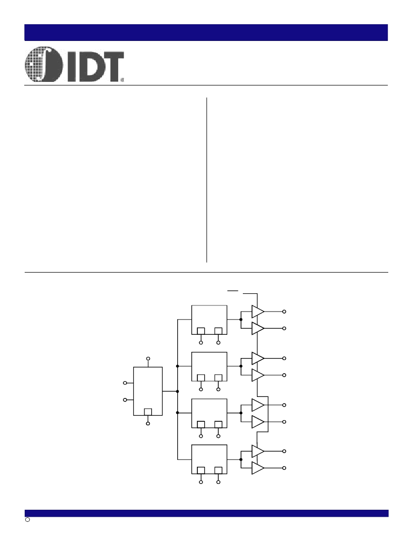
FUNCTIONAL BLOCK DIAGRAM
DESCRIPTION:
The IDT5992A is a high fanout PLL based clock driver intended for
high performance computing and data-communications applications. A
key feature of the programmable skew is the ability of outputs to lead or
lag the REF input signal. The IDT5992A has eight programmable skew
outputs in four banks of 2. Skew is controlled by 3-level input signals
that may be hard-wired to appropriate HIGH-MID-LOW levels.
The IDT5992A maintains Cypress CY7B992 compatibility while pro-
viding two additional features: Synchronous Output Enable (GND/
sOE
),
and Positive/Negative Edge Synchronization (V
DDQ
/PE). When the GND/
sOE
pin is held low, all the outputs are synchronously enabled (CY7B992
compatibility). However, if GND/
sOE
is held high, all the outputs except
3Q0 and 3Q1 are synchronously disabled.
Furthermore, when the V
DDQ
/PE is held high, all the outputs are syn-
chronized with the positive edge of the REF clock input (CY7B992 com-
patibility). When V
DDQ
/PE is held low, all the outputs are synchronized
with the negative edge of REF.
GND/sOE
1Q
0
Skew
Select
1Q
1
1F1:0
3
3
2Q
0
Skew
Select
2Q
1
2F1:0
FS
3
REF
PLL
FB
3
3Q
0
Skew
Select
3Q
1
3F1:0
3
3
4Q
0
4Q
1
Skew
Select
4F1:0
3
3
3
V
DDQ
/PE
相關PDF資料 |
PDF描述 |
|---|---|
| IDT5V9910A-2SOC | EIGHT DISTRIBUTED-OUTPUT CLOCK DRIVER|SOP|24PIN|PLASTIC |
| IDT5V991A-2JC | EIGHT DISTRIBUTED-OUTPUT CLOCK DRIVER|LDCC|32PIN|PLASTIC |
| IDT6198LE | x4 SRAM |
| IDT6198LF | x4 SRAM |
| IDT6198LRT | x4 SRAM |
相關代理商/技術參數(shù) |
參數(shù)描述 |
|---|---|
| IDT5P30017NDGI | 制造商:Integrated Device Technology Inc 功能描述:IC CLOCK GENERATOR 28QFN |
| IDT5P30017NDGI8 | 制造商:Integrated Device Technology Inc 功能描述:IC CLOCK GENERATOR 28QFN |
| IDT5P30018NBG8 | 制造商:Integrated Device Technology Inc 功能描述:IC CLOCK GENERATOR 28QFN |
| IDT5P49EE502NDGI | 制造商:Integrated Device Technology Inc 功能描述:IC CLOCK GENERATOR 20QFN |
| IDT5P49EE502NDGI8 | 制造商:Integrated Device Technology Inc 功能描述:IC CLOCK GENERATOR 28QFN |
發(fā)布緊急采購,3分鐘左右您將得到回復。