- 您現(xiàn)在的位置:買賣IC網(wǎng) > PDF目錄378613 > IDT54FCT377TE (Integrated Device Technology, Inc.) FAST CMOS OCTAL D FLIP-FLOP WITH CLOCK ENABLE PDF資料下載
參數(shù)資料
| 型號: | IDT54FCT377TE |
| 廠商: | Integrated Device Technology, Inc. |
| 英文描述: | FAST CMOS OCTAL D FLIP-FLOP WITH CLOCK ENABLE |
| 中文描述: | 快速CMOS八路D觸發(fā)器時鐘使能浮點運算 |
| 文件頁數(shù): | 2/7頁 |
| 文件大小: | 111K |
| 代理商: | IDT54FCT377TE |
6.14
2
IDT54/74FCT377T/AT/CT/DT
FAST CMOS OCTAL D FLIP-FLOP WITH CLOCK ENABLE
MILITARY AND COMMERCIAL TEMPERATURE RANGES
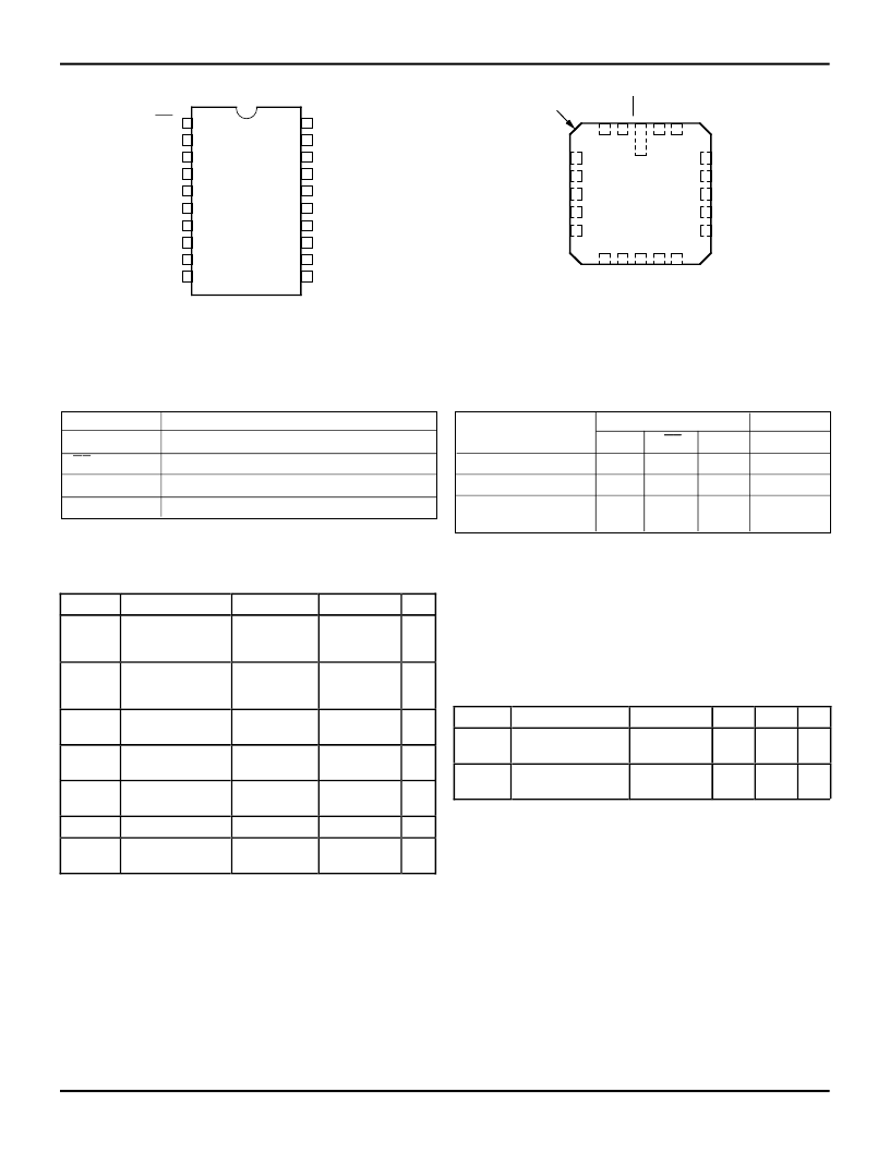
PIN CONFIGURATIONS
DIP/SOIC/QSOP/CERPACK
TOP VIEW
LCC
TOP VIEW
PIN DESCRIPTION
Pin Names
D
0
– D
7
CE
Description
Data Inputs
Clock Enable (Active LOW)
Data Outputs
Clock Pulse Input
O
0
– O
7
CP
2630 tbl 01
FUNCTION TABLE
(1)
Inputs
CE
Outputs
O
H
L
No Change
No Change
Operating Mode
Load “1”
Load “0”
Hold
CP
↑
↑
↑
H
D
h
l
X
X
l
l
h
H
NOTE:
1. H = HIGH Voltage Level
h = HIGH Voltage Level one setup time prior to the LOW-to-HIGH
Clock Transition
L = LOW Voltage Level
l
= LOW Voltage Level one setup time prior to the LOW-to-HIGH Clock
Transition
X = Don't Care
↑
= LOW-to-HIGH Clock Transition
2630 tbl 02
ABSOLUTE MAXIMUM RATINGS
(1)
Symbol
Rating
V
TERM(2)
Terminal Voltage
with Respect to
GND
V
TERM(3)
Terminal Voltage
with Respect to
GND
T
A
Operating
Temperature
T
BIAS
Temperature
Under Bias
T
STG
Storage
Temperature
P
T
Power Dissipation
CAPACITANCE
(T
A
= +25
°
C, f = 1.0MHz)
Symbol
C
IN
Parameter
(1)
Input
Capacitance
Output
Capacitance
Conditions
V
IN
= 0V
Typ.
6
Max. Unit
10
pF
C
OUT
V
OUT
= 0V
8
12
pF
NOTE:
1. This parameter is measured at characterization but not tested.
Commercial
–0.5 to +7.0
Military
–0.5 to +7.0
Unit
V
–0.5 to
V
CC
+0.5
–0.5 to
V
CC
+0.5
V
0 to +70
–55 to +125
°
C
–55 to +125
–65 to +135
°
C
–55 to +125
–65 to +150
°
C
0.5
0.5
W
I
OUT
DC Output
Current
–60 to +120 –60 to +120 mA
2630 lnk 03
2630 lnk 04
NOTES:
1. Stresses greater than those listed under ABSOLUTE MAXIMUM RAT-
INGS may cause permanent damage to the device. This is a stress rating
only and functional operation of the device at these or any other conditions
above those indicated in the operational sections of this specification is
not
implied. Exposure to absolute maximum rating conditions for
extended periods may affect reliability. No terminal voltage may exceed
V
CC
by +0.5V unless otherwise noted.
2. Input and V
CC
terminals only.
3. Outputs and I/O terminals only.
2630 drw 02
5
6
7
8
9
10
D
0
D
1
O
1
O
2
D
2
D
3
O
3
1
2
3
4
20
19
18
17
16
15
14
13
12
11
Vcc
O
7
CE
O
0
D
7
D
6
O
6
O
5
D
5
D
4
O
4
CP
GND
P20-1
D20-1
SO20-2
SO20-8
&
E20-1
INDEX
15
14
18
17
16
5
6
7
8
4
L20-2
D
0
D
1
O
1
O
2
D
2
D
3
V
C
D
7
D
6
O
6
O
5
D
5
O
3
C
D
4
G
O
4
O
0
O
7
9 10 11 12 13
3
2
1
20 19
2630 drw 03
相關(guān)PDF資料 |
PDF描述 |
|---|---|
| IDT74FCT377TE | FAST CMOS OCTAL D FLIP-FLOP WITH CLOCK ENABLE |
| IDT54FCT377TEB | HT Series Hi-Temperature Basic Switch, Single Pole Double Throw Circuitry, 2 A at 250 Vac, Overtravel Plunger Actuator, Screw Termination |
| IDT74FCT377TEB | HT Series Hi-Temperature Basic Switch, Single Pole Double Throw Circuitry, 2 A at 250 Vac, Overtravel Plunger Actuator, Screw Termination |
| IDT54FCT377TSO | FAST CMOS OCTAL D FLIP-FLOP WITH CLOCK ENABLE |
| IDT74FCT377TSO | FAST CMOS OCTAL D FLIP-FLOP WITH CLOCK ENABLE |
相關(guān)代理商/技術(shù)參數(shù) |
參數(shù)描述 |
|---|---|
| IDT54FCT521ADB | 制造商:Integrated Device Technology Inc 功能描述: |
| IDT54FCT533DB | 制造商:Integrated Device Technology Inc 功能描述: |
| IDT54FCT543ADB | 制造商:MAJOR 功能描述: |
| IDT54FCT543ATDB | 制造商:MAJOR 功能描述: |
| IDT54FCT573ADB | 制造商:Integrated Device Technology Inc 功能描述: |
發(fā)布緊急采購,3分鐘左右您將得到回復(fù)。