- 您現(xiàn)在的位置:買(mǎi)賣(mài)IC網(wǎng) > PDF目錄383094 > ICX038DLA (Sony Corporation) Diagonal 8mm (Type 1/2) CCD Image Sensor for EIA Black-and-White Video Cameras PDF資料下載
參數(shù)資料
| 型號(hào): | ICX038DLA |
| 廠商: | Sony Corporation |
| 英文描述: | Diagonal 8mm (Type 1/2) CCD Image Sensor for EIA Black-and-White Video Cameras |
| 中文描述: | 對(duì)角線(xiàn)毫米(類(lèi)型1 / 2)CCD圖像傳感器的環(huán)境影響評(píng)估黑與白錄相機(jī) |
| 文件頁(yè)數(shù): | 4/21頁(yè) |
| 文件大小: | 227K |
| 代理商: | ICX038DLA |
第1頁(yè)第2頁(yè)第3頁(yè)當(dāng)前第4頁(yè)第5頁(yè)第6頁(yè)第7頁(yè)第8頁(yè)第9頁(yè)第10頁(yè)第11頁(yè)第12頁(yè)第13頁(yè)第14頁(yè)第15頁(yè)第16頁(yè)第17頁(yè)第18頁(yè)第19頁(yè)第20頁(yè)第21頁(yè)
– 4 –
ICX038DNA
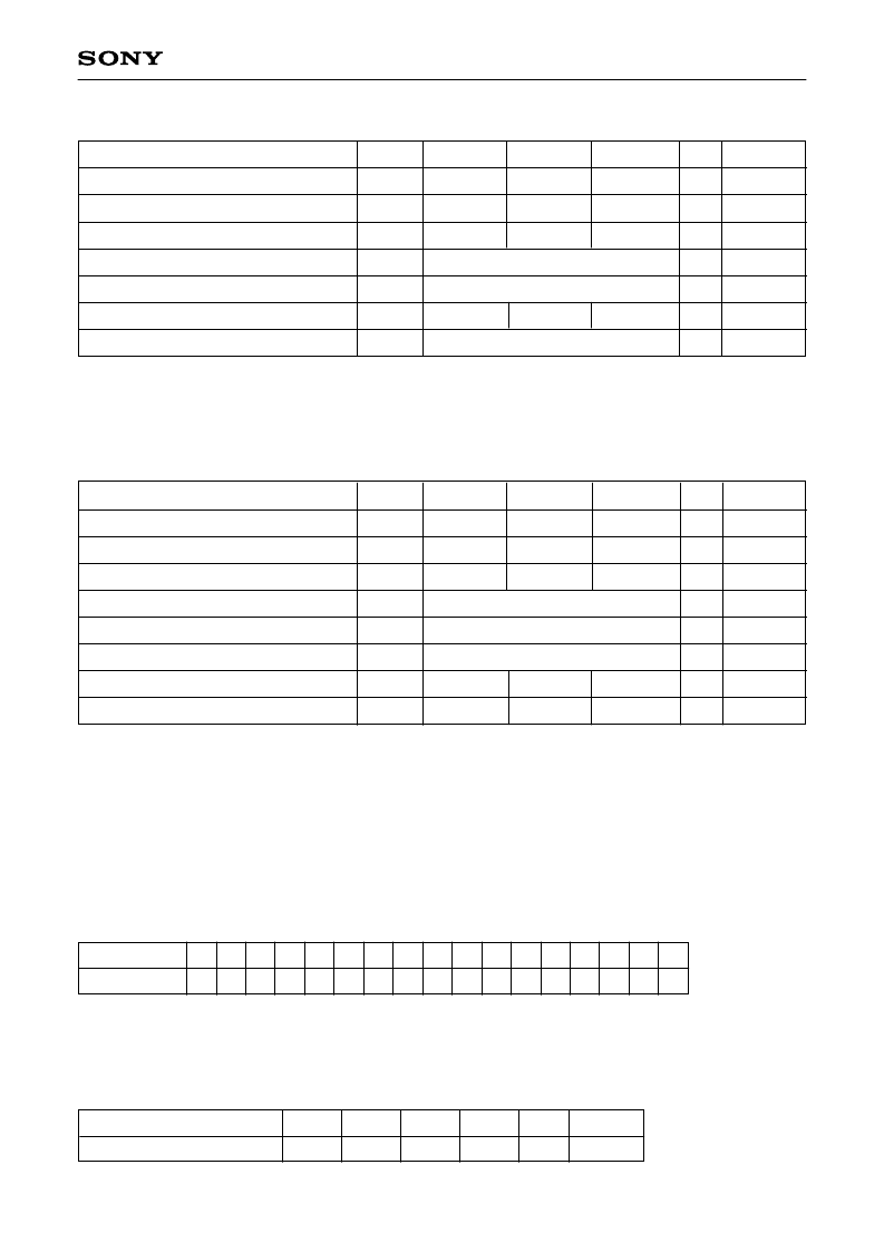
Item
V
DD
V
RD
V
GG
V
SS
V
L
V
DSUB
V
SUB
V
SUB
14.55
14.55
1.75
6.0
–3
15.0
15.0
2.0
3
4
15.45
15.45
2.25
14.0
+3
V
V
V
V
%
V
RD
= V
DD
5
5
Symbol
Min.
Typ.
Max.
Unit
Remarks
Bias Conditions 2 [when used in substrate bias external adjustment mode]
Output circuit supply voltage
Reset drain voltage
Output circuit gate voltage
Output circuit source
Protective transistor bias
Substrate bias circuit supply voltage
Substrate voltage adjustment range
Substrate voltage adjustment precision
3
V
L
setting is the V
VL
voltage of the vertical transfer clock waveform, or the same supply voltage as the V
L
power supply for the V driver should be used. (When CXD1267AN is used.)
Connect to GND or leave open.
The setting value of the substrate voltage (V
SUB
) is indicated on the back of the image sensor by a special
code. When adjusting the substrate voltage externally, adjust the substrate voltage to the indicated
voltage. The adjustment precision is ±3%. However, this setting value has not significance when used in
substrate bias internal generation mode.
4
5
V
SUB
code — one character indication
Code and optimal setting correspond to each other as follows.
DC Characteristics
Item
Output circuit supply current
I
DD
5.0
10.0
mA
Symbol
Min.
Typ.
Max.
Unit
Remarks
V
SUB
code
Optimal setting 6.0 6.5 7.0 7.5 8.0 8.5 9.0 9.5
10.0 10.5 11.0 11.5 12.0 12.5 13.0 13.5 14.0
E
f
G
h
J
K
L
m
N
P
Q
R
S
T
U
V
W
<Example> "L"
→
V
SUB
= 9.0V
Item
V
DD
V
RD
V
GG
V
SS
V
L
V
DSUB
φ
SUB
14.55
14.55
1.75
Grounded with 390
resistor
14.55
15.0
15.0
2.0
1
15.0
2
15.45
15.45
2.25
15.45
V
V
V
V
V
RD
= V
DD
Symbol
Min.
Typ.
Max.
Unit
Remarks
Bias Conditions 1 [when used in substrate bias internal generation mode]
Output circuit supply voltage
Reset drain voltage
Output circuit gate voltage
Output circuit source
Protective transistor bias
Substrate bias circuit supply voltage
Substrate clock
1
V
L
setting is the V
VL
voltage of the vertical transfer clock waveform, or the same supply voltage as the V
L
power supply for the V driver should be used. (When CXD1267AN is used.)
Do not apply a DC bias to the substrate clock pin, because a DC bias is generated within the CCD.
2
Grounded with 390
resistor
相關(guān)PDF資料 |
PDF描述 |
|---|---|
| ICX038DLB | Diagonal 8mm (Type 1/2) CCD Image Sensor for EIA Black-and-White Video Cameras |
| ICX038BNA | Diagonal 8mm (Type 1/2) CCD Image Sensor for NTSC Color Video Cameras |
| ICX038BNB | Diagonal 8mm (Type 1/2) CCD Image Sensor for NTSC Color Video Cameras |
| ICX039 | Diagonal 8mm (Type 1/2) CCD Image Sensor for CCIR Black-and-White Video Cameras |
| ICX039DNA | Diagonal 8mm (Type 1/2) CCD Image Sensor for PAL Color Video Cameras |
相關(guān)代理商/技術(shù)參數(shù) |
參數(shù)描述 |
|---|---|
| ICX038DLB | 制造商:SONY 制造商全稱(chēng):Sony Corporation 功能描述:Diagonal 8mm (Type 1/2) CCD Image Sensor for EIA Black-and-White Video Cameras |
| ICX038DNA | 制造商:SONY 制造商全稱(chēng):Sony Corporation 功能描述:Diagonal 8mm (Type 1/2) CCD Image Sensor for NTSC Color Video Cameras |
| ICX038DNB | 制造商:SONY 制造商全稱(chēng):Sony Corporation 功能描述:Diagonal 8mm (Type 1/2) CCD Image Sensor for NTSC Color Video Cameras |
| ICX039 | 制造商:SONY 制造商全稱(chēng):Sony Corporation 功能描述:Diagonal 8mm (Type 1/2) CCD Image Sensor for CCIR Black-and-White Video Cameras |
| ICX039BLA | 制造商:SONY 制造商全稱(chēng):Sony Corporation 功能描述:Diagonal 8mm (Type 1/2) CCD Image Sensor for CCIR Black-and-White Video Cameras |
發(fā)布緊急采購(gòu),3分鐘左右您將得到回復(fù)。