- 您現(xiàn)在的位置:買賣IC網(wǎng) > PDF目錄360780 > ICS9160-03 Frequency Generator and Integrated Buffer for PowerPC PDF資料下載
參數(shù)資料
| 型號: | ICS9160-03 |
| 英文描述: | Frequency Generator and Integrated Buffer for PowerPC |
| 中文描述: | 頻率發(fā)生器和集成緩沖器為PowerPC |
| 文件頁數(shù): | 2/7頁 |
| 文件大小: | 240K |
| 代理商: | ICS9160-03 |
2
ICS9160-03
Preliminary Product Preview
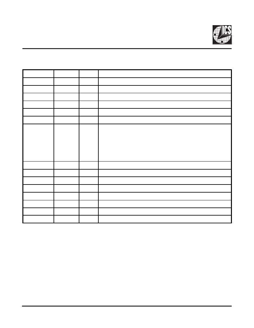
Pin Descriptions
* Frequencies assuming an input or crystal of 14.318 MHz.
** Device provides 18pF load capacitance for crystal.
PIN NUMBER
PIN NAME
TYPE
DESCRIPTION
XTAL or external reference frequency input. This input includes XTAL load
capacitance and feedback bias for a 10-30 MHz XTAL.**
XTAL output which includes XTAL load capacitance.**
2
X1
IN
3
1
4
X2
OUT
VDDX
GNDX
FS(0:2)
PWR
XTAL oscillator circuit and REFCLK output power supplies.
5, 6, 7
IN
Frequency selection address pins. These inputs have pull-ups.
Processor clock outputs which are a multiple of the input reference frequency as
shown in the table below.
PCLK power supplies. VDDP powers the internal PCLK PLL and the
PCLK(0:3) outputs.
Serial stop clock data is clocked in on the falling edge of BCLK. A total of 15 bits
must be clocked in using the following protocol. SDATA is sampled on the falling
edge of BCLK, so the data generator should change data on the rising edge of
BCLK to ensure proper communication. SDATA must be low for one BCLK period
as a start bit. The next 15 rising edges of BCLK will clock data in serially. The
16th clock enables the serial data to take effect. Outputs associated with serial data
bits that are a one will continue without interruption. Clocks associated with serial
data bits that are a zero will be stopped in the low state glitch-free, that is, no short
clocks with the exception of REFCLK and KEYBD which do not stop. This input
has an internal pull-up device.
Stop clock control pins used for glitch-free start and stop of the clock outputs as
described in the table on the next page. These inputs have internal pull-up devices.
Buffered copy of the crystal reference frequency.
Bus clock outputs having selectable frequency based on the FS(0:2) inputs (see
table on next page).
BCLK power supplies. VSSB and VDDB power BCLK(0:6).
Fixed clock power supplies. VSSF and VDDF power GRAPHIC, FLOPPY and
KEYBD outputs plus the fixed clock PLL.
The floppy clock output operates at 24 MHz..*
8, 9, 11, 12
PCLK(0:3)
OUT
10, 17
13
VDDP
GNDP
PWR
14
SDATA
IN
15, 16
STOP(0:1)
IN
18
REFCLK
OUT
19, 21, 22, 24,
25, 27, 28
20
23
26
29
30
BCLK(0:6)
GNDB
VDDB
GNDF
VDDF
FLOPPY
OUT
PWR
PWR
OUT
31
KEYBD
OUT
The keyboard clock output operates at 12 MHz.*
32
GRAPHIC
OUT
The graphics system clock output operates at 40 MHz.*
相關(guān)PDF資料 |
PDF描述 |
|---|---|
| ICS9160M-03 | Frequency Generator and Integrated Buffer for PowerPC |
| ICS9161A | Low-Power High-Performance Impact<TM> PAL<R> Circuits 28-PLCC 0 to 75 |
| ICS9161A-01CW16 | Dual Programmable Graphics Frequency Generator |
| ICS9169C-232 | Frequency Generator for Pentium⑩ Based Systems |
| ICS9169C-27 | Frequency Generator for Pentium™ Based Systems |
相關(guān)代理商/技術(shù)參數(shù) |
參數(shù)描述 |
|---|---|
| ICS9160M-03 | 制造商:ICS 制造商全稱:ICS 功能描述:Frequency Generator and Integrated Buffer for PowerPC |
| ICS9161A | 制造商:ICS 制造商全稱:ICS 功能描述:Dual Programmable Graphics Frequency Generator |
| ICS9161A-01CN16 | 制造商:未知廠家 制造商全稱:未知廠家 功能描述:Video/Graphics Clock Generator |
| ICS9161A-01CW | 制造商:ICS 功能描述: 制造商:INT_CIR_SYS 功能描述: |
| ICS9161A-01CW16 | 功能描述:IC FREQUENCY GENERATOR 16-SOIC RoHS:否 類別:集成電路 (IC) >> 時鐘/計時 - 專用 系列:- 標準包裝:1,500 系列:- 類型:時鐘緩沖器/驅(qū)動器 PLL:是 主要目的:- 輸入:- 輸出:- 電路數(shù):- 比率 - 輸入:輸出:- 差分 - 輸入:輸出:- 頻率 - 最大:- 電源電壓:3.3V 工作溫度:0°C ~ 70°C 安裝類型:表面貼裝 封裝/外殼:28-SSOP(0.209",5.30mm 寬) 供應(yīng)商設(shè)備封裝:28-SSOP 包裝:帶卷 (TR) 其它名稱:93786AFT |
發(fā)布緊急采購,3分鐘左右您將得到回復(fù)。