- 您現(xiàn)在的位置:買賣IC網(wǎng) > PDF目錄360780 > ICS9158-07 50/125 PVC LC-SC 2M DUPLEX ASSEM PDF資料下載
參數(shù)資料
| 型號: | ICS9158-07 |
| 英文描述: | 50/125 PVC LC-SC 2M DUPLEX ASSEM |
| 中文描述: | 頻率發(fā)生器和集成緩沖器 |
| 文件頁數(shù): | 4/7頁 |
| 文件大?。?/td> | 167K |
| 代理商: | ICS9158-07 |
4
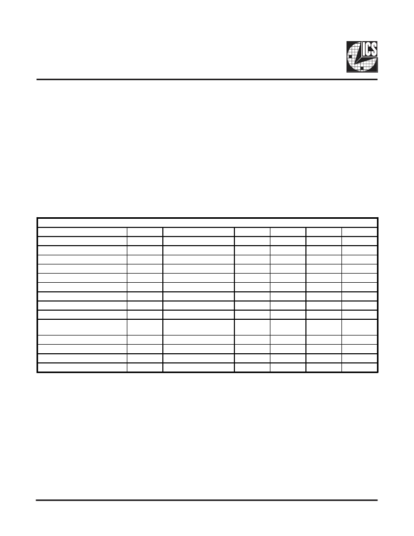
ICS9158-03
Electrical Characteristics at 5V
V
DD
= +5V±10%, T
A
=0°C to 70°C unless otherwise stated
Absolute Maximum Ratings
AVDD, VDD referenced to GND . . . . . . . . . . . . . . . . 7V
Operating temperature under bias. . . . . . . . . . . . . . . . 0°C to +70°C
Storage temperature . . . . . . . . . . . . . . . . . . . . . . . . . . -40°C to +150°C
Voltage on I/O pins referenced to GND. . . . . . . . . . . GND -0.5V to VDD +0.5V
Power dissipation . . . . . . . . . . . . . . . . . . . . . . . . . . . . 0.5 Watts
Stresses above those listed under Absolute Maximum Ratings may cause permanent damage to the device. This is a stress
rating only and functional operation of the device at these or any other conditions above those indicated in the operational
sections of the specifications is not implied. Exposure to absolute maximum rating conditions for extended periods may affect
product reliability.
DC Characteristics
TEST CONDITIONS
PARAMETER
SYMBOL
V
IL
V
IH
I
IL
I
IH
V
OL
V
OH
I
OL
I
OH
I
DD
MIN
TYP
MAX
0.8
UNITS
V
V
μA
μA
V
V
mA
mA
mA
Input Low Voltage
Input High Voltage
Input Low Current
Input High Current
Output Low Voltage
Output High Voltage
1
Output Low Current
1
Output High Current
1
Supply Current
Output Frequency Change over
Supply and Temperature
1
Short circuit current
1
Pull-up resistor value
1
Input Capacitance
1
Load Capacitance
1
2.0
-20
-5
V
IN
=0V (Pull-up)
V
IN
=V
DD
I
OL
=20.0mA
I
OH
=-30mA
V
OL
=0.8V
V
OH
=2.0V
No load, 66 MHz
With respect to typical
frequency
Each output clock
Input pin
Except X1, X2
Pins X1, X2
5
0.25
3.5
65
-55
67
0.4
2.4
45
-35
100
F
D
0.002
0.01
%
I
SC
R
PU
C
i
C
L
25
56
680
mA
k
pf
pf
8
20
Note 1: Parameter is guaranteed by design and characterization. Not 100% tested in production.
相關(guān)PDF資料 |
PDF描述 |
|---|---|
| ICS9158-07M | 50/125 PVC LC-SC 3M DUPLEX ASSEM |
| ICS9159-05 | 50/125 PVC ST-ST 2M DUPLEX ASSEM |
| ICS9159F-12 | Frequency Generator and Buffers for Mobile Pentium™ Systems |
| ICS9159-06 | 50/125 PVC ST-ST 3M DUPLEX ASSEM |
| ICS9159-07 | 50/125 PVC ST-ST 5M DUPLEX ASSEM |
相關(guān)代理商/技術(shù)參數(shù) |
參數(shù)描述 |
|---|---|
| ICS9158-07M | 制造商:ICS 制造商全稱:ICS 功能描述:Frequency Generator and Integrated Buffer |
| ICS9158-07N | 制造商:未知廠家 制造商全稱:未知廠家 功能描述:CPU System Clock Generator |
| ICS9158M01 | 制造商:未知廠家 制造商全稱:未知廠家 功能描述:Peripheral IC |
| ICS9158N01 | 制造商:未知廠家 制造商全稱:未知廠家 功能描述:Peripheral IC |
| ICS9159-02M | 制造商:未知廠家 制造商全稱:未知廠家 功能描述:Peripheral IC |
發(fā)布緊急采購,3分鐘左右您將得到回復(fù)。