- 您現(xiàn)在的位置:買賣IC網(wǎng) > PDF目錄360768 > ICS843003AI01 FEMTOCLOCKS-TM CRYSTAL-TO-3.3V LVPECL FREQUENCY SYNTHESIZER PDF資料下載
參數(shù)資料
| 型號(hào): | ICS843003AI01 |
| 英文描述: | FEMTOCLOCKS-TM CRYSTAL-TO-3.3V LVPECL FREQUENCY SYNTHESIZER |
| 中文描述: | FEMTOCLOCKS -商標(biāo)晶體至3.3的LVPECL頻率合成器 |
| 文件頁(yè)數(shù): | 1/13頁(yè) |
| 文件大小: | 198K |
| 代理商: | ICS843003AI01 |
當(dāng)前第1頁(yè)第2頁(yè)第3頁(yè)第4頁(yè)第5頁(yè)第6頁(yè)第7頁(yè)第8頁(yè)第9頁(yè)第10頁(yè)第11頁(yè)第12頁(yè)第13頁(yè)
843003AGI-01
www.icst.com/products/hiperclocks.html
REV. A MAY 26, 2005
1
Integrated
Circuit
Systems, Inc.
ICS843003I-01
F
EMTO
C
LOCKS
C
RYSTAL
-
TO
-3.3V LVPECL
F
REQUENCY
S
YNTHESIZER
PRELIMINARY
G
ENERAL
D
ESCRIPTION
The ICS843003I-01 is a 3 differential output
LVPECL Synthesizer designed to generate
Ethernet reference clock frequencies and is a
member of the HiPerClocks amily of high per-
formance clock solutions from ICS. Using a
19.53125MHz or 25MHz, 18pF parallel resonant crystal, the
following frequencies can be generated based on the
settings of 4 frequency select pins (DIV_SEL[A1:A0],
DIV_SEL[B1:B0]): 625MHz, 312.5MHz, 156.25MHz, and
125MHz. The 843003I-01 has 2 output banks, Bank A with
1 differential LVPECL output pair and Bank B with 2 dif-
ferential LVPECL output pairs.
The two banks have their own dedicated frequency se-
lect pins and can be independently set for the frequen-
cies mentioned above. The ICS843003I-01 uses ICS’ 3rd
generation low phase noise VCO technology and can
achieve 1ps or lower typical rms phase jitter, easily meet-
ing Ethernet jitter requirements. The ICS843003I-01 is
packaged in a small 24-pin TSSOP package.
F
EATURES
Three 3.3V LVPECL outputs on two banks, A Bank with
one LVPECL pair and B Bank with 2 LVPECL output pairs
Using a 19.53125MHz or 25MHz crystal, the two output
banks can be independently set for 625MHz, 312.5MHz,
156.25MHz or 125MHz
Selectable crystal oscillator interface or LVCMOS/LVTTL
single-ended input
VCO range: 490MHz to 680MHz
RMS phase jitter @ 156.25MHz (1.875MHz - 20MHz):
0.53ps (typical)
3.3V output supply mode
-40°C to 85°C ambient operating temperature
HiPerClockS
ICS
P
IN
A
SSIGNMENT
1
2
3
4
5
6
7
8
9
10
11
12
ICS843003I-01
24-Lead TSSOP
4.40mm x 7.8mm x 0.92mm
package body
G Package
Top View
QA0
DIV_SELB0
VCO_SEL
MR
V
CCO
_
A
QA0
nQA0
CLK_ENB
CLK_ENA
FB_DIV
V
CCA
V
CC
DIV_SELA0
DIV_SELB1
V
CCO
_
B
QB0
nQB0
QB1
nQB1
XTAL_SEL
TEST_CLK
XTAL_IN
XTAL_OUT
V
EE
DIV_SELA1
24
23
22
21
20
19
18
17
16
15
14
13
0
1
0
1
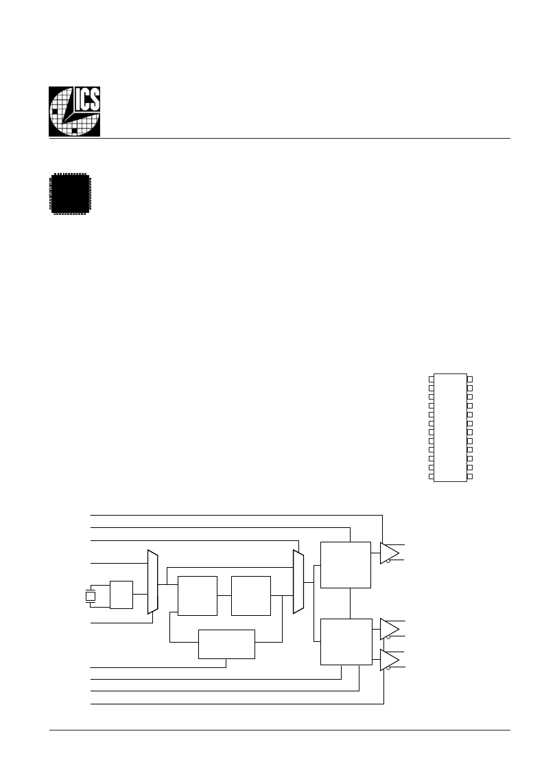
Phase
Detector
VCO
0 = ÷25 (default)
1 = ÷32
0 0 ÷1
0 1 ÷2
1 0 ÷3
1 1 ÷4
(default)
0 0 ÷2
0 1 ÷4
1 0 ÷5
1 1 ÷8
(default)
FB_DIV
OSC
CLK_ENA
DIV_SELA[1:0]
VCO_SEL
TEST_CLK
XTAL_IN
XTAL_OUT
XTAL_SEL
FB_DIV
DIV_SELB[1:0]
MR
CLK_ENB
nQA0
QB0
nQB0
QB1
nQB1
Pulldown
Pulldown
Pullup
Pullup
Pullup
Pullup
Pulldown
Pullup
Pullup
B
LOCK
D
IAGRAM
The Preliminary Information presented herein represents a product in prototyping or pre-production. The noted characteristics are based on initial
product characterization. Integrated Circuit Systems, Incorporated (ICS) reserves the right to change any circuitry or specifications without notice.
相關(guān)PDF資料 |
PDF描述 |
|---|---|
| ICS843003I-01 | FEMTOCLOCKS-TM CRYSTAL-TO-3.3V LVPECL FREQUENCY SYNTHESIZER |
| ICS843004-01 | FEMTOCLOCKS-TM CRYSTAL-TO- 3.3V LVPECL FREQUENCY SYNTHESIZER |
| ICS843004A01 | FEMTOCLOCKS-TM CRYSTAL-TO- 3.3V LVPECL FREQUENCY SYNTHESIZER |
| ICS843004AG-01 | FEMTOCLOCKS-TM CRYSTAL-TO- 3.3V LVPECL FREQUENCY SYNTHESIZER |
| ICS843004AG-01T | FEMTOCLOCKS-TM CRYSTAL-TO- 3.3V LVPECL FREQUENCY SYNTHESIZER |
相關(guān)代理商/技術(shù)參數(shù) |
參數(shù)描述 |
|---|---|
| ICS843003I-01 | 制造商:ICS 制造商全稱:ICS 功能描述:FEMTOCLOCKS-TM CRYSTAL-TO-3.3V LVPECL FREQUENCY SYNTHESIZER |
| ICS843003I-09 | 制造商:IDT 制造商全稱:Integrated Device Technology 功能描述:FEMTOCLOCKS? CRYSTAL-TO-3.3V LVPECL FREQUENCY SYNTHESIZER |
| ICS843004 | 制造商:ICS 制造商全稱:ICS 功能描述:FEMTOCLOCKS⑩ LVCMOS/CRYSTAL-TO- 3.3V LVPECL FREQUENCY SYNTHESIZER |
| ICS843004-01 | 制造商:ICS 制造商全稱:ICS 功能描述:FEMTOCLOCKS-TM CRYSTAL-TO- 3.3V LVPECL FREQUENCY SYNTHESIZER |
| ICS843004-02 | 制造商:ICS 制造商全稱:ICS 功能描述:CRYSTAL-TO-3.3V LVPECL FREQUENCY SYNTHESIZER |
發(fā)布緊急采購(gòu),3分鐘左右您將得到回復(fù)。