- 您現(xiàn)在的位置:買賣IC網(wǎng) > PDF目錄67689 > ICS843002CY-31T (SPECTRUM CONTROL INC) 700 MHz, OTHER CLOCK GENERATOR, PQFP64 PDF資料下載
參數(shù)資料
| 型號: | ICS843002CY-31T |
| 廠商: | SPECTRUM CONTROL INC |
| 元件分類: | 時鐘產(chǎn)生/分配 |
| 英文描述: | 700 MHz, OTHER CLOCK GENERATOR, PQFP64 |
| 封裝: | 10 X 10 MM, 1 MM HEIGHT, EXPOSED PAD, MS-026BCD, TQFP-64 |
| 文件頁數(shù): | 10/27頁 |
| 文件大小: | 270K |
| 代理商: | ICS843002CY-31T |
第1頁第2頁第3頁第4頁第5頁第6頁第7頁第8頁第9頁當前第10頁第11頁第12頁第13頁第14頁第15頁第16頁第17頁第18頁第19頁第20頁第21頁第22頁第23頁第24頁第25頁第26頁第27頁
843002CY-31
www.icst.com/products/hiperclocks.html
REV. B NOVEMBER 22, 2005
18
Integrated
Circuit
Systems, Inc.
ICS843002-31
700MHZ FEMTOCLOCKSVCXO BASED
FREQUENCY TRANSLATOR AND JITTER ATTENUATOR
PRELIMINARY
C
P =
C
S
20
NOTES ON SETTING THE VALUE OF C
P
As another general rule, the following relationship should be
maintained between components C
S and CP in the loop filter:
C
P establishes a second pole in the VCXO PLL loop filter.
For higher damping factors (> 1), calculate the value of C
P
based on a C
S value that would be used for a damping
factor of 1. This will minimize baseband peaking and loop
instability that can lead to output jitter.
C
P also dampens VCXO PLL input voltage modulation by the
charge pump correction pulses. A C
P value that is too low will
result in increased output phase noise at the phase detector
frequency due to this. In extreme cases where input jitter is
high, charge pump current is high, and C
P is too small, the
VCXO PLL input voltage can hit the supply or ground rail
resulting in non-linear loop response.
The best way to set the value of C
P is to use the filter response
software available from ICS (please refer to the following
section). C
P should be increased in value until it just starts
affecting the passband peak.
NOTES ON EXTERNAL CRYSTAL LOAD CAPACITORS
In the loop filter schematic diagram, capacitors are shown
from pin 62 to ground and pin 63 to ground. These are
optional crystal load capacitors which can be used to cen-
ter tune the external pullable crystal (the crystal frequency
can only be lowered by adding capacitance, it cannot be
raised). Note that the addition of external load capacitors
will decrease the crystal pull range and the Kvco value.
LOOP FILTER RESPONSE SOFTWARE
Online tools to calculate loop filter response can be found at
www.icst.com.
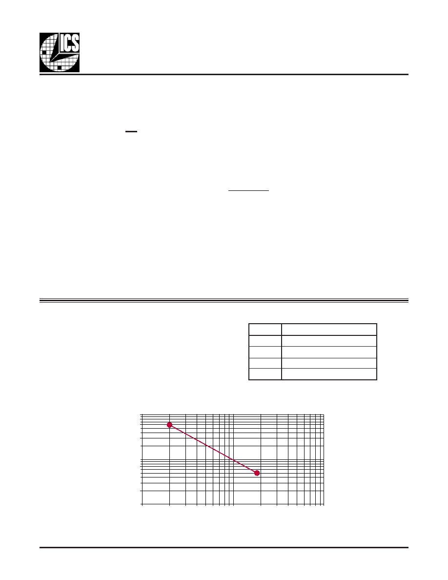
NOTES ON SETTING CHARGE PUMP CURRENT
The recommended range for the charge pump current is
50
μA to 500μA. Below 50μA, loop filter charge leakage,
due to PCB or capacitor leakage, can become a problem.
This loop filter leakage can cause locking problems, output
clock cycle slips, or low frequency phase noise.
As can be seen in the loop bandwidth and damping factor
equations or by using the filter response software available
from ICS, increasing charge pump current (I
CP) increases
both bandwidth and damping factor.
R
T
E
S
I
(
t
n
e
r
u
C
p
m
u
P
e
g
r
a
h
C
P
C )
K
6
.
7
1A
5
.
2
6
K
8
.
8A
5
2
1
K
4
.
4A
0
5
2
K
2
.
2A
0
5
1E-3
100E-6
10E-6
1k
10k
100k
RSET, Ω
I CP
,Amps
FIGURE 2. CHARGE PUMP CURRENT VS. VALUE OF R
SET
(EXTERNAL RESISTOR) GRAPH
CHARGE PUMP CURRENT, EXAMPLE SETTINGS
相關PDF資料 |
PDF描述 |
|---|---|
| ICS843003AGLF | 700 MHz, OTHER CLOCK GENERATOR, PDSO24 |
| ICS843004AG-01LFT | 156.25 MHz, OTHER CLOCK GENERATOR, PDSO24 |
| ICS843004AG-02LFT | 637.5 MHz, OTHER CLOCK GENERATOR, PDSO24 |
| ICS843004AG-02LF | 680 MHz, OTHER CLOCK GENERATOR, PDSO24 |
| ICS843004AGI-01 | 170 MHz, OTHER CLOCK GENERATOR, PDSO24 |
相關代理商/技術參數(shù) |
參數(shù)描述 |
|---|---|
| ICS843002I | 制造商:ICS 制造商全稱:ICS 功能描述:FEMTOCLOCKS-TM CRYSTAL-TO-3.3V, 2.5V LVPECL FREQUENCY SYNTHESIZER |
| ICS843002I-01 | 制造商:ICS 制造商全稱:ICS 功能描述:FEMTOCLOCKS-TM CRYSTAL-TO- 3.3V, 2.5V LVPECL FREQUENCY SYNTHESIZER |
| ICS843002I-40 | 制造商:ICS 制造商全稱:ICS 功能描述:175MHZ, FEMTOCLOCKS-TM VCXO BASED SONET/SDH JITTER ATTENUATOR |
| ICS843002I-41 | 制造商:ICS 制造商全稱:ICS 功能描述:700MHz, FEMTOCLOCKS-TM VCXO BASED SONET/SDH JITTER ATTENUATOR |
| ICS843002I-72 | 制造商:IDT 制造商全稱:Integrated Device Technology 功能描述:FEMTOCLOCKS⑩ VCXO BASED WCDMA CLOCK GENERATOR/JITTER ATTENUATOR |
發(fā)布緊急采購,3分鐘左右您將得到回復。