- 您現(xiàn)在的位置:買賣IC網(wǎng) > PDF目錄360752 > ICS614M-01 2 CHANNEL COMPONENT VIDEOSPLITTER/SWITCHER PDF資料下載
參數(shù)資料
| 型號(hào): | ICS614M-01 |
| 英文描述: | 2 CHANNEL COMPONENT VIDEOSPLITTER/SWITCHER |
| 中文描述: | 16引腳英特爾圖形時(shí)鐘源 |
| 文件頁數(shù): | 3/4頁 |
| 文件大小: | 65K |
| 代理商: | ICS614M-01 |
ICS614-01
16 pin Intel Graphics Clock Source
MDS 614-01 B
Integrated Circuit Systems 525 Race Street San Jose CA95126 (408) 295-9800tel (408) 295-9818fax
3
Revision 020199
Printed 11/14/00
ICRO
C
LOC K
PRELIMINARY INFORMATION
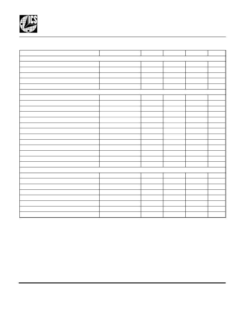
Parameter
ABSOLUTE MAXIMUM RATINGS (note 1)
Supply voltage, VDD
Inputs and Clock Outputs
Ambient Operating Temperature
Soldering Temperature
Storage temperature
DC CHARACTERISTICS (VDD = 5.0V unless noted)
Operating Voltage, VDD
Operating Voltage, VDDIO
Input High Voltage, VIH, X1 pin only
Input Low Voltage, VIL, X1 pin only
Input High Voltage, VIH
Input Low Voltage, VIL
Output High Voltage, VOH
Output Low Voltage, VOL
Output High Voltage, VOH, CMOS level
Operating Supply Current, IDD
Short Circuit Current
Input Capacitance
VIN, VCXO control voltage
AC CHARACTERISTICS (VDD = 5.0V unless noted)
Input Frequency
Input Crystal Accuracy
Output Clock Accuracy (all but PAL square pixel) Given exact input
Output Clock Rise Time
Output Clock Fall Time
Output Clock Duty Cycle
Maximum Absolute Jitter, short term
Maximum Jitter, one sigma
Conditions
Minimum
Typical
Maximum
Units
Referenced to GND
Referenced to GND
7
V
V
C
C
C
-0.5
0
VDD+0.5
70
260
150
Max of 10 seconds
-65
4.50
3.13
3.5
5.50
VDD
V
V
V
V
V
V
V
V
V
2.5
2.5
1.5
2
0.8
IOH=-25mA
IOL=25mA
IOH=-8mA
No Load
Each output
OE, select pins
2.4
0.4
VDD-0.4
35
±100
5
mA
mA
pF
V
0
3
27.000000
0
MHz
ppm
ppm
ns
ns
%
ps
ps
30
1
1.5
1.5
60
0.8 to 2.0V, no load
0.8 to 2.0V, no load
At VDD/2
40
±150
50
Electrical Specifications
Notes:
1. Stresses beyond those listed under Absolute Maximum Ratings could cause permanent damage to the device. Prolonged
exposure to levels above the operating limits but below the Absolute Maximums may affect device reliability.
相關(guān)PDF資料 |
PDF描述 |
|---|---|
| ICS614M-01T | 2 CHANNEL DVI SPLITTER |
| ICS614-01 | 16 pin Intel Graphics Clock Source |
| ICS615 | Set-Top Box Clock Source |
| ICS615M | RES 41.2 OHM 1/10W 1% 0603 SMD |
| ICS615MT | Set-Top Box Clock Source |
相關(guān)代理商/技術(shù)參數(shù) |
參數(shù)描述 |
|---|---|
| ICS614M-01T | 制造商:ICS 制造商全稱:ICS 功能描述:16 pin Intel Graphics Clock Source |
| ICS615 | 制造商:ICS 制造商全稱:ICS 功能描述:Set-Top Box Clock Source |
| ICS615M | 制造商:ICS 制造商全稱:ICS 功能描述:Set-Top Box Clock Source |
| ICS615MT | 制造商:ICS 制造商全稱:ICS 功能描述:Set-Top Box Clock Source |
| ICS620-01 | 制造商:ICS 制造商全稱:ICS 功能描述:Digital Still Camera Clock Source |
發(fā)布緊急采購(gòu),3分鐘左右您將得到回復(fù)。