- 您現(xiàn)在的位置:買(mǎi)賣(mài)IC網(wǎng) > PDF目錄383090 > ICL7673CPA (INTERSIL CORP) Automatic Battery Back-Up Switch PDF資料下載
參數(shù)資料
| 型號(hào): | ICL7673CPA |
| 廠(chǎng)商: | INTERSIL CORP |
| 元件分類(lèi): | 電源管理 |
| 英文描述: | Automatic Battery Back-Up Switch |
| 中文描述: | 1-CHANNEL POWER SUPPLY SUPPORT CKT, PDIP8 |
| 封裝: | PLASTIC, MS-001-BA, DIP-8 |
| 文件頁(yè)數(shù): | 5/7頁(yè) |
| 文件大?。?/td> | 144K |
| 代理商: | ICL7673CPA |
3-85
supply voltage. A low-impedance capacitor such as a
0.047
μ
F disc ceramic can be used to reduce the rate-of-rise.
Status Indicator Outputs
The N-Channel open drain output transistors can be used to
indicate which supply is connected, or can be used to drive
external PNP transistors to increase the power switching
capability of the circuit. When using external PNP power
transistors, the output current is limited by the beta and
thermal characteristics of the power transistors. The
application section details the use of external PNP
transistors.
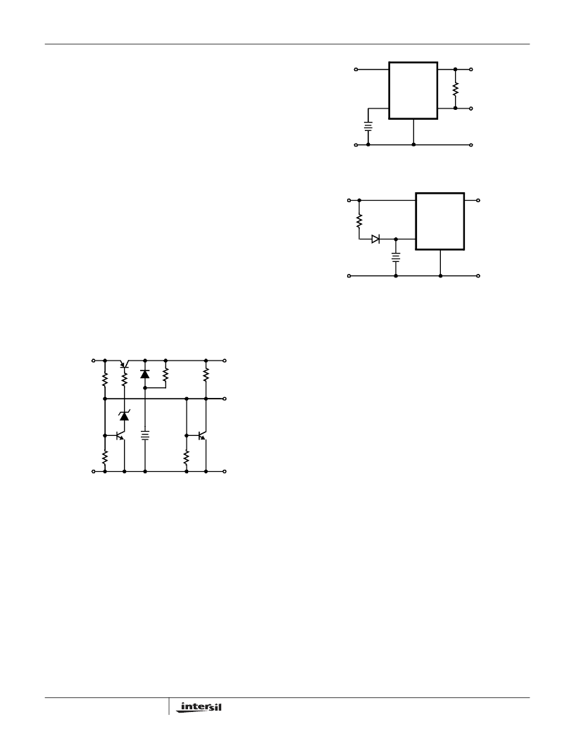
Applications
A typical discrete battery backup circuit is illustrated in Figure
6. This approach requires several components, substantial
printed circuit board space, and high labor cost. It also
consumes a fairly high quiescent current. The ICL7673
battery backup circuit, illustrated in Figure 7, will often replace
such discrete designs and offer much better performance,
higher reliability, and lower system manufacturing cost. A
trickle charge system could be implemented with an additional
resistor and diode as shown in Figure 8. A complete low
power AC to regulated DC system can be implemented using
the ICL7673 and ICL7663S micropower voltage regulator as
shown in Figure 9.
Applications for the ICL7673 include volatile semiconductor
memory storage systems, real-time clocks, timers, alarm
systems, and over/under the voltage detectors. Other
systems requiring DC power when the master AC line supply
fails can also use the ICL7673.
A typical application, as illustrated in Figure 12, would be a
microprocessor system requiring a 5V supply. In the event of
primary supply failure, the system is powered down, and a
3V battery is employed to maintain clock or volatile memory
data. The main and backup supplies are connected to V
P
and V
S
, with the circuit output V
O
supplying power to the
clock or volatile memory. The ICL7673 will sense the main
supply, when energized, to be of greater potential than V
S
and connect, via its internal MOS switches, V
P
to output V
O
.
The backup input, V
S
will be disconnected internally. In the
event of main supply failure, the circuit will sense that the
backup supply is now the greater potential, disconnect V
P
from V
O
, and connect V
S
.
Figure 11 illustrates the use of external PNP power
transistors to increase the power switching capability of the
circuit. In this application the output current is limited by the
beta and thermal characteristics of the power transistors.
If hysteresis is desired for a particular low power application,
positive feedback can be applied between the input V
P
and
open drain output S
BAR
through a resistor as illustrated in
Figure 12. For high power applications hysteresis can be
applied as shown in Figure 13.
The ICL7673 can also be used as a clipping circuit as
illustrated in Figure 14. With high impedance loads the
circuit output will be nearly equal to the greater of the two
input signals.
+5V
PRIMARY
DC POWER
GND
NiCAD
BATTERY
STACK
V
O
+5V OR
+3V
STATUS
INDICATOR
FIGURE 6. DISCRETE BATTERY BACKUP CIRCUIT
V
P
V
O
V
S
GND
Pbar
8
2
1
6
V
O
+5V OR +3V
R
I
STATUS
INDICATOR
LITHIUM
BATTERY
GND
+5V
PRIMARY
SUPPLY
4
+
-
FIGURE 7. ICL7673 BATTERY BACKUP CIRCUIT
V
P
V
O
V
S
GND
8
2
1
V
+5V OR +3V
RECHARGEABLE
BATTERY
GND
+5V
PRIMARY
SUPPLY
4
R
C
+
-
FIGURE 8. APPLICATION REQUIRING RECHARGEABLE
BATTERY BACKUP
ICL7673
相關(guān)PDF資料 |
PDF描述 |
|---|---|
| ICL7673 | Automatic Battery Back-Up Switch(自動(dòng)后備電池開(kāi)關(guān)) |
| ICL8013 | 1MHz, Four Quadrant Analog Multiplier |
| ICL8013CCTX | 1MHz, Four Quadrant Analog Multiplier |
| ICL8013BCTX | 1MHz, Four Quadrant Analog Multiplier |
| ICL8048BCJE | Log Amplifier |
相關(guān)代理商/技術(shù)參數(shù) |
參數(shù)描述 |
|---|---|
| ICL7673CPA136 | 制造商:Harris Corporation 功能描述: |
| ICL7673CPAZ | 功能描述:電池管理 W/ANNEAL BATTERY BAC KUPSWITCH8PDIPCOM RoHS:否 制造商:Texas Instruments 電池類(lèi)型:Li-Ion 輸出電壓:5 V 輸出電流:4.5 A 工作電源電壓:3.9 V to 17 V 最大工作溫度:+ 85 C 最小工作溫度:- 40 C 封裝 / 箱體:VQFN-24 封裝:Reel |
| ICL7675IPA | 制造商:Rochester Electronics LLC 功能描述:- Bulk 制造商:Harris Corporation 功能描述: |
| ICL8001 | 制造商:INTERSIL 制造商全稱(chēng):Intersil Corporation 功能描述:N-CHANNEL JFET |
| ICL8001G | 功能描述:LED照明驅(qū)動(dòng)器 SGL STAGE FLYBCK PFC CTLR LED LIGHT APP RoHS:否 制造商:STMicroelectronics 輸入電壓:11.5 V to 23 V 工作頻率: 最大電源電流:1.7 mA 輸出電流: 最大工作溫度: 安裝風(fēng)格:SMD/SMT 封裝 / 箱體:SO-16N |
發(fā)布緊急采購(gòu),3分鐘左右您將得到回復(fù)。